Here is the input stage, constant voltage and constant current = constant power .....
WOW, JFET Baxandall combined input pair, if it's stable we can incorporate it in. What do you think Sonnya? It looks great.

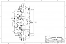
TSSA Basic - cascoded Baxandall input pairs
I did a little homework.")
Here they're, real Baxandall input pairs cascoded with JFETs in TSSA Basic.
In the post #339 you've drawn Sziklai pairs.
Which of these compound input pair transistors to take to perform better? Good question.
Sonnya by this version of TSSA Basic you can finally omit extra bias/offset CCSs.
Post 330.
Substitute the input bipolars with Baxandall pairs and then you have my circuit
I did a little homework.
Here they're, real Baxandall input pairs cascoded with JFETs in TSSA Basic.
In the post #339 you've drawn Sziklai pairs.
Which of these compound input pair transistors to take to perform better? Good question.
Sonnya by this version of TSSA Basic you can finally omit extra bias/offset CCSs.
Attachments
Actually i was going to write this morning about the Sziklai pair.
We need to test it. A solution would be to add it to the layout. If we decide it should not be there because of listening test we can just replace the 1K resistor with an 0R resistor and remove the extra transistor.
The same is the case with the extra CCS for bias and offset.
We need to test it. A solution would be to add it to the layout. If we decide it should not be there because of listening test we can just replace the 1K resistor with an 0R resistor and remove the extra transistor.
The same is the case with the extra CCS for bias and offset.
Bad news.
While showering i was thinking why i did not use jfet... (am i the only one thinking audio?).
The is no complementary jfets, so the vgs value is different on p-jfet and n-jfet leading to different voltage drop across the bjt's that we cascode.
So they are not biased the same way and they will heat up to different temperatures and then we start getting drift in the circuit.
Also the hFE versus IC changes with the VCE drop.
But maybe Andrej could measure the vCE difference in his CCS???
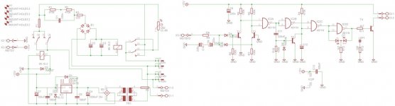
To continue on TSSA BIGBT HP building here, following LC suggestion, a new board with soft start and speaker protection circuit that drive TLP627 at +12V
Marc
Looks good Idefixes, CL-90 involved to soft start the amp.
As you could saw in my inrush current oscilloscope plot, the secondary relay which shorts NTC (3 Ap on plot), fires 0,68 s after the first relay. Shortening delay time let's say to 0,5 s, would cause the secondary relay to short at higher current app. 5 Ap, longer delay will help the contacts to shorten lower primary current. I suggest you to set delay to app. 1 s since you'll charge a lot higher capacitance in the power supply.
Otherwise circuit is OK, just be very careful to have enough isolation distance from the mains conducting tracks.
Otherwise circuit is OK, just be very careful to have enough isolation distance from the mains conducting tracks.
Have you detect one specific place where it seems not enough?
Marc
Bad news.
While showering i was thinking why i did not use jfet... (am i the only one thinking audio?).
The is no complementary jfets, so the vgs value is different on p-jfet and n-jfet leading to different voltage drop across the bjt's that we cascode.
So they are not biased the same way and they will heat up to different temperatures and then we start getting drift in the circuit.
Also the hFE versus IC changes with the VCE drop.
But maybe Andrej could measure the vCE difference in his CCS???
Nothing to worry about Sonnya
I did consider that data before drawing sch, I did measure Vce ie. Vgs in my CCSs and it was always in a range 1,8-2,2 V. If JFET's drain current (Id at Vgs=0) selection is made than Vgs can be well within preferred limits.
At Banxadall pair input BJT's Vce=Vbe(second BJT) so not Vgs dependant, bias current is set by 1k resistor, as this forces app. Ic=(Vgs-Vbe)/1 k=1,5 mA input bias setting.
At Sziklai pair Vce of the input transistor is Vce=Vgs-Vbe, bias current is app. Ic=Vbe/680 ohm=1 mA
At both pairs bias conditions can be well defined, it is just our decision which pair we'll coose. Sziklai pair is stable as Darlington is, Banxadall pair according to Homemodder experiences from reallity, also is. So we have to decide firmly on better performance as the input transistor in this case.
Have you detect one specific place where it seems not enough?
Marc
Not really, looks fine.
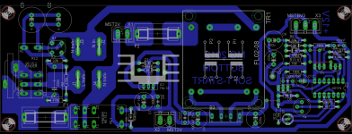
Only that I would put six 6,3 mm male fastons on PCB:
- first pair of fastons for mains input: L in (phase input), N in (neutral input)
- second pair of fastons for mains1 out: L1 out (left channel transformer primary - phase ), N1 out (left channel transformer primary - neutral)
- third pair of fastons for mains2 out: L2 out (right channel transformer primary - phase ), N2 out (right channel transformer primary - neutral)
This would help to connect Channel's transformers primaries faster and more reliable to the Soft Start PCB.
I tend to agree on this one.
We are increasing the complexity on the input pair, but we do nothing to ease the load from the mosfets. I think this is more important.
It just have to be a simple EF.
Guys, please be aware that this is still TSSA Basic, two stages amplifier, strictly following first post schematic, only that its single stages are improved with sophisticated compound parts.
Up to now, we transformed single input BJT's to Sziklai/Banxadall pairs, replaced resistor current injectors with high impedance CC source/sink. So for the output stage we can also implement some sort of compound BJT/MOSFET, the only condition is that we stay out of any extra thermal compensation circuit, as TSSA Basic from post #1 is free of.
Not really, looks fine.
Only that I would put six 6,3 mm male fastons on PCB:
- first pair of fastons for mains input: L in (phase input), N in (neutral input)
- second pair of fastons for mains1 out: L1 out (left channel transformer primary - phase ), N1 out (left channel transformer primary - neutral)
- third pair of fastons for mains2 out: L2 out (right channel transformer primary - phase ), N2 out (right channel transformer primary - neutral)
This would help to connect Channel's transformers primaries faster and more reliable to the Soft Start PCB.
Faston are already on PCB. But one main since i will have one soft start/speaker protection per amp (2 independant case). Main two could be used for fisrt stage +10V power supply...i see what i can do.
marc
Faston are already on PCB. But one main since i will have one soft start/speaker protection per amp (2 independant case). Main two could be used for fisrt stage +10V power supply...i see what i can do.
marc
OK, one PCB per mono amp, that's clear.
Less PCB-s, less wires, less interferences, the better.
- Home
- Amplifiers
- Solid State
- TSSA - The Simplest Symmetrical Amplifier