andy_c said:
Yikes! I looked at the 3b, and it's a strange topology. I must admit I can't think of anything very kind to say about it.
My reaction was about the same, it was almost painful to look at the 3B schematic at first. Then I took another look at the performance and amazingly the distortion is very low typically .00x even at 20 kHz which is something not often seen in power amps. Now I'm wondering if there's something to be learned from an amp that goes against the common beliefs but performs so well. My view now is that perhaps the Bryston is like a Porsche 911 having roots in the VW.
I built the Tigersaurous many years ago and the 3B looks very much like a hybrid of that design and the Tiger .01. I hesitated to build it because I had experience with the Universal Tiger oscillating, but also knew that it was probably on the edge because it only went unstable under unusual conditions. The Tigersaurous added emitter degeneration in the diff amp so we reasoned that it had lower open loop gain and therefore better gain margin. My older brother who was in engineering school explained this to me at the time. The Tigersaurous also used a cap from the VAS to the - input of the diff amp which Leach later suggested was better to reduce TIM. Some say this was used as far back as the 60s.
It's interesting that the 3B does not use emitter degeneration in the diff amp, but uses heavy degeneration in the VAS, this is what was done in the Universal Tiger and goes against what is preached by Leach, Self etc., however a Cdom configuration is usually assumed and there is no Cdom in the Bryston or Tiger amps. I'm wondering if there's something to be learned from these designs since the HF distortion (TIM/SID?) problems seem to come from a high gain diff amp combined with a large (slow forward loop) Cdom. I would lean toward adding degeneration in the diff amp and less in the VAS.
It's interesting that these designs have voltage gain in the driver/output stage which fits well with cascoding the VAS and which makes up for the reduced voltage swing.
I'm thinking of a Self diff amp/VAS, perhaps with cascoding (diff amp and VAS) and emitter degeneration on the VAS for a more linear open loop amplifier that requires less feedback, with a (Universal Tiger) gain of 2 output stage to make up for the loss in VAS swing. Less feedback will allow the Cdom cap to be reduced or in other words the dominant pole increased in freq.
My goal is a simple amp topology that has low distortion across the audio band, it seems that most Cdom configurations do not accomplish this because of reduced forward gain at HF. I revisited Self's site and he seems to claim low .00x distortion even at 20 kHz so perhaps he's there, I'll have to take a closer look at how he does it.
andy_c said:
In a couple of places, they're introducing a zero in the open-loop gain to compensate for a pole. For example, the capacitor in parallel with R40 in the 3b does this. I've tried this technique in the lab when I was in college in the '70s. What I found was that one could get good pole-zero cancellation experimentally with a given transistor. But then, after replacing the transistor with another of the same vendor and type, the cancellation was way off. The idea of course is to get stability by looking at the problem purely in the frequency domain. But there are a number of articles published in the 1970s where the authors discuss how attempts at pole-zero cancellation pretty much hose the settling time. Anybody who has ever played around on the bench with composite op-amps (which also use pole-zero cancellation techniques), trying to get a combination of low offset and noise, and high slew rate knows that the settling time of these configurations is really awful.
I should probably just keep quiet, as this is sounding like a rant...
Yes, I also wondered about those caps but perhaps they're just attempting to push the HF performance in the right direction and not provide perfect cancellation. I'm guessing, giving them the benefit of the doubt, that the amp is stable without them, adding them perhaps improves the stability, somewhat and makes it more tolerant of output device variation. I doubt that they have much impact anywere near the audio band to harm closed loop settling time. JMO I don't see your comments as a rant, the design is very different and odd in many ways.
andy_c said:
You might be interested in looking at the thread "Amplifier Topology Subjective Effects". There's some interesting discussion there. That was before I realized just how good the Lin topology could be made to be.
Nice work in that thread, very interesting, it's taking some time to read but well worth it, some real brainiacs on here, LOL. I've also been interested in using cascodes on the diff amp and VAS and recently have been thinking how the output gain of the Universal Tiger topology would make up for the loss of voltage swing with cascoding. Seems to be a natural combination. I might rough out a concept for this design.
Gain output stage
I once "discovered" (some 15 years back) an interesting output stage topology that provides as much voltage gain as you want and behaves fairly well. Only to find out of course (here) it was already invented and goes by some proper name I don't recall.
Looking only at the upper half (the lower is complementary symetric) you start with a small npn capable of withstanding a little more than half the rail to rail voltage. load the collector with a resistor to +V and the base (gate) of an pnp (p chann) power device. Return from the collector (drain) which is the output, a feedback resistor to the first transistor's emitter, *and* from there to ground. You may add an upstream emitter resistor for the first transistor to improve linearity and ease biasing. This configuration provides a high open loop gain from input to output so the closed loop gain is very nearly the feedback divider ratio.
You may notice the topology is exactly current feedback, being the input transistor in cascode (common base) configuration for the feedback loop.
I do not know why this topology is not more widespread, except perhaps for an ingrained concept that output stages should always operate in emitter (source) follower mode to provide low output impedance (something feedback does anyway in a well designed project).
I have simulated and tested this with good results, as long as of course global feedback is also used in the complete system.
The combination of fairly good input impedance, and voltage gain make this circuit for an excellent match to a high performance low distortion audio opamp as driver.
In fact I am working on such project and expect to post results if something interesting comes by.
Rodolfo
mikeks said:
NE5532/3/4 do not use double-pole compensation...
Then... how do you explain ,the wrinkle , in the open loop gain near 200 KhZ?
That produce a transition from the 27 Mhz inicial gain bandwidth product , for the 10 MhZ after the wrinkle ....
Correction
Andy, you mentioned the cap across R40. I thought (above) that you were referring to a different cap, now I see in the SST schematics that I think you mean the 22 pF, C18 for example.
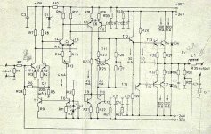
What I believe is going on is that the VAS has heavy emitter degeneration, a whoping 2.2 K and therefore it will have high input impedance, low gain, and a high break point. The high input impedance allows the diff amp to act as a voltage amp with high gain since there's no emitter degeneration and it is probably the dominant pole in the amp. C18 is an attempt to push the VAS pole even higher and improve stability, as far as I can tell.
PB2 said:
Yes, I also wondered about those caps but perhaps they're just attempting to push the HF performance in the right direction and not provide perfect cancellation. I'm guessing, giving them the benefit of the doubt, that the amp is stable without them, adding them perhaps improves the stability, somewhat and makes it more tolerant of output device variation. I doubt that they have much impact anywere near the audio band to harm closed loop settling time. JMO I don't see your comments as a rant, the design is very different and odd in many ways.
Andy, you mentioned the cap across R40. I thought (above) that you were referring to a different cap, now I see in the SST schematics that I think you mean the 22 pF, C18 for example.
What I believe is going on is that the VAS has heavy emitter degeneration, a whoping 2.2 K and therefore it will have high input impedance, low gain, and a high break point. The high input impedance allows the diff amp to act as a voltage amp with high gain since there's no emitter degeneration and it is probably the dominant pole in the amp. C18 is an attempt to push the VAS pole even higher and improve stability, as far as I can tell.
Re: Gain output stage
Hi Rodolfo,
I'm not sure if I'm following your schematic, is it anything like the schematic in the first post of this thread, this is the Universal Tiger that I mentioned:
http://www.diyaudio.com/forums/showthread.php?s=&threadid=41926
ingrast said:I once "discovered" (some 15 years back) an interesting output stage topology that provides as much voltage gain as you want and behaves fairly well. Only to find out of course (here) it was already invented and goes by some proper name I don't recall.
Looking only at the upper half (the lower is complementary symetric) you start with a small npn capable of withstanding a little more than half the rail to rail voltage. load the collector with a resistor to +V and the base (gate) of an pnp (p chann) power device. Return from the collector (drain) which is the output, a feedback resistor to the first transistor's emitter, *and* from there to ground. You may add an upstream emitter resistor for the first transistor to improve linearity and ease biasing. This configuration provides a high open loop gain from input to output so the closed loop gain is very nearly the feedback divider ratio.
Rodolfo
Hi Rodolfo,
I'm not sure if I'm following your schematic, is it anything like the schematic in the first post of this thread, this is the Universal Tiger that I mentioned:
http://www.diyaudio.com/forums/showthread.php?s=&threadid=41926
Re: Re: Gain output stage
Yes, basically the same but with one less resistor.
Rodolfo
PB2 said:
Hi Rodolfo,
I'm not sure if I'm following your schematic, is it anything like the schematic in the first post of this thread, this is the Universal Tiger that I mentioned:
http://www.diyaudio.com/forums/showthread.php?s=&threadid=41926
Yes, basically the same but with one less resistor.
Rodolfo
Attachments
Correction
I forgot that the original Leach did not use a Cdom cap, the later II,3,4 versions did but the value is very small. Just seeing the cap there in later schematics made me think that he used a large value, I was mistaken. He seems to be shooting for wide open loop bandwidth yet the amp still has rising HF distortion, probably because it is a low feedback amp and there's not enough feedback to reduce the HF non-linearities. Has anyone found a simple way to lower the HF distortion in the Leach?
PB2 said:
Yes, this makes sense and it's interesting to note that the distortion in the Leach amp is .006% at 20 Hz, starts to rise from about 1 kHz and reaches .29 % at 20 kHz partly due to Cdom compensation as can be seen in Figure 4:
http://users.ece.gatech.edu/~mleach/lowtim/bckgrnd.html
Even .29% is low, and I don't get alarmed about it but the technical challenge to have low distortion even at high frequencies is interesting. It is interesting to contrast this with the Bryston amps which have very low distortion across the audio band.
I forgot that the original Leach did not use a Cdom cap, the later II,3,4 versions did but the value is very small. Just seeing the cap there in later schematics made me think that he used a large value, I was mistaken. He seems to be shooting for wide open loop bandwidth yet the amp still has rising HF distortion, probably because it is a low feedback amp and there's not enough feedback to reduce the HF non-linearities. Has anyone found a simple way to lower the HF distortion in the Leach?
Re: Re: Re: Gain output stage
Hi Rudolfo.
Something like this...(output stage )
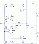
http://www.audiofanatic.it/Schemi/Tipo/Stato_solido/finali/pic_finaliSS/120W_MOS_IRF9540_540.jpg
ingrast said:
Yes, basically the same but with one less resistor.
Rodolfo
Hi Rudolfo.
Something like this...(output stage )
http://www.audiofanatic.it/Schemi/Tipo/Stato_solido/finali/pic_finaliSS/120W_MOS_IRF9540_540.jpg
Re: Re: Re: Re: Gain output stage
Exactly (except I should go for a higher than 3x gain as in this case).
I wonder why is it that this output stage is not popular.
Rodolfo
Tube_Dude said:
Hi Rudolfo.
Something like this...(output stage )
http://www.audiofanatic.it/Schemi/Tipo/Stato_solido/finali/pic_finaliSS/120W_MOS_IRF9540_540.jpg
Exactly (except I should go for a higher than 3x gain as in this case).
I wonder why is it that this output stage is not popular.
Rodolfo
Hi, PB2,
Can I have the Otala paper too? lumanauw@bdg.centrin.net.id
Does anyone has this cct : Lohstroh, J. & Otala, M.: An audio power amplifier for ultimate quality requirements. AES 44th Convention - Rotterdam 1973
Can I have the Otala paper too? lumanauw@bdg.centrin.net.id
Does anyone has this cct : Lohstroh, J. & Otala, M.: An audio power amplifier for ultimate quality requirements. AES 44th Convention - Rotterdam 1973
lumanauw said:Hi, PB2,
Can I have the Otala paper too? lumanauw@bdg.centrin.net.id
Does anyone has this cct : Lohstroh, J. & Otala, M.: An audio power amplifier for ultimate quality requirements. AES 44th Convention - Rotterdam 1973
Hi,
I sent you Otala's preprint that we've been discussing. I have this paper from the IEEE Transactions IIRC, but not scanned: Lohstroh, J. & Otala, M.: An audio power amplifier for ultimate quality requirements
This online schematic looks like what was in that paper as far as I remember:
http://home.online.no/~tsandstr/Otala amp 1973, original.htm
Interesting that it is inverting and has 3 gain stages.
Re: Re: Re: Re: Re: Gain output stage
Hi Rudolfo
Because it has a High intrinsic open loop output impedance.
As the openloop output impedance is high , if you have a load with a phase shift (thats what you have with a speaker)the feedback will be not in phase wih the input signal,but with the phase of the load inprinted in it!
Second and more important ,all the EMF of the peaker is not dissipated , in the low output impedance of the output stage , but will be connected to the input stage where it can intermodulate with the input signal...puting in another way the amplifier will be subjected
at two input signals...the normal input signal and a delayed and distorted that comes from the speaker...is obvious that one will intermodulate with the other.
In your circuit , the low output impedance is obtained from the feedback . But as the open loop is very high the reactions from the speakers "fell free" for reaching the input LTP ...
This is nothing new as Matti Otalla have call it interface intermodulation distortion ( AES Convention ,Hamburg , March 1978 ).
ingrast said:
Exactly (except I should go for a higher than 3x gain as in this case).
I wonder why is it that this output stage is not popular.
Rodolfo
Hi Rudolfo
Because it has a High intrinsic open loop output impedance.
As the openloop output impedance is high , if you have a load with a phase shift (thats what you have with a speaker)the feedback will be not in phase wih the input signal,but with the phase of the load inprinted in it!
Second and more important ,all the EMF of the peaker is not dissipated , in the low output impedance of the output stage , but will be connected to the input stage where it can intermodulate with the input signal...puting in another way the amplifier will be subjected
at two input signals...the normal input signal and a delayed and distorted that comes from the speaker...is obvious that one will intermodulate with the other.
In your circuit , the low output impedance is obtained from the feedback . But as the open loop is very high the reactions from the speakers "fell free" for reaching the input LTP ...
This is nothing new as Matti Otalla have call it interface intermodulation distortion ( AES Convention ,Hamburg , March 1978 ).
More comments on the Bryston 3B schematic
I had a look at this again to try to compute the frequency of the zero introduced by C18. Since the voltage gain of a common-emitter amp is approximately -ZC/ZE and ZE = R40/(1+sR40C18) then the zero is at s = -1/(R40C18). This comes out to about 3.3 MHz. Looks like it's just attempting to cancel out some non-dominant pole. So you're right, it's at too high a frequency to have much affect on the settling time. The dominant pole looks like it's set at the junctions of the collectors of Q21 and Q22 via C13, C15 and the Miller-multiplied C27 and C28 all appearing in parallel.
Another thing that threw me off at first was that the open-loop gain appeared somewhat uncontrolled, such that the stability couldn't be easily controlled. It took me a while to see what Rodolfo saw right away - that the output stage has a gain of 3 via the feedback loop formed by R25 and R28. If we assume the gain is completely controlled by this local feedback loop, threre's a pole in this gain introduced by C7 and R25 at 169 kHz, and a zero at 3 times this frequency or 508 kHz.
I think I understand better now why the distortion of this amp is so low. There's lots of local feedback in the output stage because of R25 and R28, which covers up the class B crossover distortion. Then the overall feedback reduces it still further. There's lots of local feedback in the 3x gain output stage because the impedance seen by the collector of Q27 is very large (since the high side of R32 is bootstrapped to the emitter of Q2). This gives the 3x gain stage a pretty high loop gain it seems. It also looks like there's a variant of two-pole compensation going on. There's the dominant pole mentioned above, plus the additional pole created by C7 and R25, then the zero created by C7 and the parallel combination of R25 and R28.
The disadvantage I see to the "feedback amp within a feedback amp" is stability with capacitive loads. With a capacitive load, the inner feedback amp might have a degraded phase margin, giving a closed-loop gain with complex poles. Complex poles can give peaking in the amplitude response and a sudden increase in phase lag with frequency. Now put this in an overall feedback loop, and the overall loop gain at high frequencies has a peak in the amplitude response at the same time the phase is dropping like a rock. Not good for stability!
PB2 said:Andy, you mentioned the cap across R40. I thought (above) that you were referring to a different cap, now I see in the SST schematics that I think you mean the 22 pF, C18 for example.
What I believe is going on is that the VAS has heavy emitter degeneration, a whoping 2.2 K and therefore it will have high input impedance, low gain, and a high break point. The high input impedance allows the diff amp to act as a voltage amp with high gain since there's no emitter degeneration and it is probably the dominant pole in the amp. C18 is an attempt to push the VAS pole even higher and improve stability, as far as I can tell.
I had a look at this again to try to compute the frequency of the zero introduced by C18. Since the voltage gain of a common-emitter amp is approximately -ZC/ZE and ZE = R40/(1+sR40C18) then the zero is at s = -1/(R40C18). This comes out to about 3.3 MHz. Looks like it's just attempting to cancel out some non-dominant pole. So you're right, it's at too high a frequency to have much affect on the settling time. The dominant pole looks like it's set at the junctions of the collectors of Q21 and Q22 via C13, C15 and the Miller-multiplied C27 and C28 all appearing in parallel.
Another thing that threw me off at first was that the open-loop gain appeared somewhat uncontrolled, such that the stability couldn't be easily controlled. It took me a while to see what Rodolfo saw right away - that the output stage has a gain of 3 via the feedback loop formed by R25 and R28. If we assume the gain is completely controlled by this local feedback loop, threre's a pole in this gain introduced by C7 and R25 at 169 kHz, and a zero at 3 times this frequency or 508 kHz.
I think I understand better now why the distortion of this amp is so low. There's lots of local feedback in the output stage because of R25 and R28, which covers up the class B crossover distortion. Then the overall feedback reduces it still further. There's lots of local feedback in the 3x gain output stage because the impedance seen by the collector of Q27 is very large (since the high side of R32 is bootstrapped to the emitter of Q2). This gives the 3x gain stage a pretty high loop gain it seems. It also looks like there's a variant of two-pole compensation going on. There's the dominant pole mentioned above, plus the additional pole created by C7 and R25, then the zero created by C7 and the parallel combination of R25 and R28.
The disadvantage I see to the "feedback amp within a feedback amp" is stability with capacitive loads. With a capacitive load, the inner feedback amp might have a degraded phase margin, giving a closed-loop gain with complex poles. Complex poles can give peaking in the amplitude response and a sudden increase in phase lag with frequency. Now put this in an overall feedback loop, and the overall loop gain at high frequencies has a peak in the amplitude response at the same time the phase is dropping like a rock. Not good for stability!
Re: Re: Re: Re: Re: Gain output stage
Hi Rodolfo,
There are probably several reasons why output stages with gain are not used more often - most probably due to historical reasons, valid or not. This is my speculation on the issue:
Some of the Tiger amplifiers are well known with a strong negative reputation for oscillation.
The elementary thinking that the output stage should have the highest current gain possible, and that followers are more stable. However, it's well known that followers with long wires, poor decoupling, lacking base stoppers, oscillate very easily.
The thinking that output stages requiring large high current devices are slow and followers provide the highest bandwidth.
Output stages with gain allow the designer to select a compromise between gain, bandwidth, and linearity just as with any other gain stage. Indeed, Self shows that the CFP offers better performance than a follower when compensated back to unity gain. I don't see any reasons why a gain of 2 - 5 cannot provide excellent performance and stability, in fact it is demonstrated in the Brystons.
Pete B.
ingrast said:
Exactly (except I should go for a higher than 3x gain as in this case).
I wonder why is it that this output stage is not popular.
Rodolfo
Hi Rodolfo,
There are probably several reasons why output stages with gain are not used more often - most probably due to historical reasons, valid or not. This is my speculation on the issue:
Some of the Tiger amplifiers are well known with a strong negative reputation for oscillation.
The elementary thinking that the output stage should have the highest current gain possible, and that followers are more stable. However, it's well known that followers with long wires, poor decoupling, lacking base stoppers, oscillate very easily.
The thinking that output stages requiring large high current devices are slow and followers provide the highest bandwidth.
Output stages with gain allow the designer to select a compromise between gain, bandwidth, and linearity just as with any other gain stage. Indeed, Self shows that the CFP offers better performance than a follower when compensated back to unity gain. I don't see any reasons why a gain of 2 - 5 cannot provide excellent performance and stability, in fact it is demonstrated in the Brystons.
Pete B.
PB2, thanks for the papers. I cannot open the Otala's "ultimate HiFi" amp. http://home.online.no/~tsandstr/Ota... original.htm
Could you send it also?
After reading them (I dont understand the mathematics part) it seems they are talking about input stage nonlinearity (BJT especially) that contributes the most to the distortions fo the whole amplifier.
This is what I got after reading them (as DIYer)
Barrie G in his "Hawaii" article, writes an interesting approach. If the output is perfectly sinusoidal, what kind of input needed to make the output like that. Problem arises with BJT differential, because it takes very little change (20mV) to make 20V full sinusoidal in output. And that 20mV signal could be not sinusoidal to make the output good sinusoidal. This means the whole amp is not linear, because what is in to the amp is different shape to what happens from the output. This is with OL mode.
I know that many nature curves (hyperbolic, exponential, etc) are "tried" tobe approached by mathematic equations. But they dont fit 100% compared with measurement. Is the bipolar model here (the GM curve) is exactly the same shape as if it was measured? That bipolar GM formula is used for base of papers.
I read that bipolars is Current driven (Ib). But here, the IC is approached by VBE function, not Ib. Is this valid?
Back to input stage. In transistor, besides putting RE, local degeneration can be made by putting large R (1M-100K) from collector to base. Why the effort made to lower GM in bipolar differential here only using RE? Can the C-B or B-E resistance used in differential?
Hi, Andy C,
Which cct you are discussing about?
lumanauw said:Hi, Andy C,
Which cct you are discussing about?
Hi lumanauw,
It is the Bryston 3B schematic located at http://www.bryston.ca/schemprod.html. These are really interesting schematics because they're using some innovative and unusual techniques. They had me completely confused when I first looked at them, but I think I understand them now.
Just shoot me an email if you want any of Otala's AES papers.
Re: Re: Re: Re: Re: Re: Gain output stage
I agree, and it is a fact of life entrenched design practices are usually not challenged.
The argument of usuallly poor high frequency performance of power devices has lost some ground though with the advent of power MOSFETS.
I believe an interesting path to do some research is to perform simulations substituting the customary resistive load with the T-S model of a typical good speaker, including the mechanical EMF generator. This way stability issues not readily apparent with resistive loads can be investigated.
I am now in the midst of an important high performance project about which I hope to be able to present results, so do not have time to work out the above proposal. Any takers?
Rodolfo
PB2 said:
Hi Rodolfo,
There are probably several reasons why output stages with gain are not used more often - most probably due to historical reasons, valid or not. This is my speculation on the issue:
Some of the Tiger amplifiers are well known with a strong negative reputation for oscillation.
The elementary thinking that the output stage should have the highest current gain possible, and that followers are more stable. However, it's well known that followers with long wires, poor decoupling, lacking base stoppers, oscillate very easily.
The thinking that output stages requiring large high current devices are slow and followers provide the highest bandwidth.
Output stages with gain allow the designer to select a compromise between gain, bandwidth, and linearity just as with any other gain stage. Indeed, Self shows that the CFP offers better performance than a follower when compensated back to unity gain. I don't see any reasons why a gain of 2 - 5 cannot provide excellent performance and stability, in fact it is demonstrated in the Brystons.
Pete B.
I agree, and it is a fact of life entrenched design practices are usually not challenged.
The argument of usuallly poor high frequency performance of power devices has lost some ground though with the advent of power MOSFETS.
I believe an interesting path to do some research is to perform simulations substituting the customary resistive load with the T-S model of a typical good speaker, including the mechanical EMF generator. This way stability issues not readily apparent with resistive loads can be investigated.
I am now in the midst of an important high performance project about which I hope to be able to present results, so do not have time to work out the above proposal. Any takers?
Rodolfo
Hi, AndyC
Thanks for the offer. I still dont know which paper, since Otala writes about many topics.
Finally, I can get the Otala amp.
I tought the main issue to make good sounding amp is low OL gain, high OL bandwith and input stage that can take quite big voltage input.
Looking at the Otala amp, he uses 3 stages front stage (not the output stage yet). The first and second is differential, and the VAS is having current mirror.
How can this be called low OL gain? I make amp with one differential input stage and current mirrored VAS (not with second differential), the sound is having too much gain (from my personal opinion). So it must be more of that in Otala amp.
And I notice the output is using L-R. This is one indication of possible oscilation (typical of too high OL gain)
Actually, what is Otala's main thinking that some people considered as "the start" of good sounding audio amps? Low OL gain seems not the one. Or Otala is not about making good sounding amp, just advoiding TIM?
Attachments
- Status
- This old topic is closed. If you want to reopen this topic, contact a moderator using the "Report Post" button.
- Home
- Amplifiers
- Solid State
- Thoughts Concerning Cordell, Otala, and Gilbert papers