Terry, the voltage readings in your post #367 look good and it seems the input stage is working as intended, except that one side of the current mirror has saturated. Without seeing voltage readings at other circuit nodes of the amp I can only guess the global feedback loop is in an open state, and because no DC is fed back to the back side of the input pair, the current mirror is thrown out of balance due to the very high gain of the input stage, hence the saturation. The problem is unlikely with the input stage itself, but somewhere down stream.
Last edited:
FYI, I added the ground wires but there was no change. I realize that this layout is probably not ideal for noise but the voltages and current should work. Quite the mystery.
I am sorry to hear that.
I can't see the ceramic 220pF C0G(NP0) C4 and C19 soldered directly on the drivers base - collector pins on the board back side. Did you added those caps? Other question is, I see that you use two resistor for R5, what value you used?
Regarding this layout, it's just opposite, this should be better noise wise with less power interference to the input side, so this layout should be more advanced then the double layer one.
BR Damir
I believe you are right. The feed back circuit has little or no current because the + side of the VAS is not turning on. Today I was able to turn the bias all the way up and get some bias on the output. With the bias up as far as it will go, the VAS is 1V on the + side and -12V on the - side of the VBE multiplier. I will try to sit down tomorrow and record all of the voltages at each transistor. If there is something else you would like to see, please let me know and I will try to get it for you.Terry, the voltage readings in your post #367 look good and it seems the input stage is working as intended, except that one side of the current mirror has saturated. Without seeing voltage readings at other circuit nodes of the amp I can only guess the global feedback loop is in an open state, and because no DC is fed back to the back side of the input pair, the current mirror is thrown out of balance due to the very high gain of the input stage, hence the saturation. The problem is unlikely with the input stage itself, but somewhere down stream.
I am sorry to hear that.
I can't see the ceramic 220pF C0G(NP0) C4 and C19 soldered directly on the drivers base - collector pins on the board back side. Did you added those caps? Other question is, I see that you use two resistor for R5, what value you used?
Regarding this layout, it's just opposite, this should be better noise wise with less power interference to the input side, so this layout should be more advanced then the double layer one.
BR Damir
Hi Damir,
The C0G caps are added on top of the board right in front of the heatsink. I drilled holes and tied the legs to the proper pins on the drivers. R5 is two 20K resistors in parallel. I just measured to be sure and I have 10k there.
Thanks, Terry
Terry, I think we are getting close to the bug. 13v across a Vbe multiplier sounds very wrong. I would double check resistance value of R24, R40, and R47. Please NEVER turn P1 all the way up, as there should be a fixed resistor in series with P1, to prevent the Vbe multiplier from putting out a hazardous high voltage, that has been omitted. Always turn P1 back to high resistance end and go from there. The Vbe multiplier is supposed to have a voltage output anywhere between 3.5V and 4.2V, measured across C97.
I'd also make sure that Q2 and Q19 were not mounted backwards. The footprint outline of these two transistors are facing the wrong way in the layout drawing.
I'd also make sure that Q2 and Q19 were not mounted backwards. The footprint outline of these two transistors are facing the wrong way in the layout drawing.
Last edited:
Terry, I think we are getting close to the bug. 13v across a Vbe multiplier sounds very wrong. I would double check resistance value of R24, R40, and R47. Please NEVER turn P1 all the way up, as there should be a fixed resistor in series with P1, to prevent the Vbe multiplier from putting out a hazardous high voltage, that has been omitted. Always turn P1 back to high resistance end and go from there. The Vbe multiplier is supposed to have a voltage output anywhere between 3.5V and 4.2V, measured across C97.
I'd also make sure that Q2 and Q19 were not mounted backwards. The footprint outline of these two transistors are facing the wrong way in the layout drawing.
Yes Nattawa I think you are right. From the photo on the page #338 both transistors Q21 and Q19 are mounted backwards. On the layout the transistor pins are marked correctly but the transistor body shape is turned by 180 degree. Sorry for this layout fault, I was checking it many times and could not noticed that. Here is corrected layout.
BR Damir
Attachments
![DADO-TT-TMC-7-2-i.LAY].jpg](/community/data/attachments/429/429328-b0a3d51c267a87c5933a8029c25897be.jpg)
Hi Damir, thanks for the confirmation. I went to the post 338 as you pointed and it appears in the photo that Q21 and Q19 are indeed backwards installed. That probably explained why we have an open global feedback loop. Hopefully this gets terry a Champagne break.
Terry, please do not forget turning P1 all the way back to its high resistance end prior to next powering up, or you may witness the unholy magic smoke.
Terry, please do not forget turning P1 all the way back to its high resistance end prior to next powering up, or you may witness the unholy magic smoke.
Last edited:
I had hoped fresh eyes would help. I will make the changes and get back to you. Seems like I'm always the sucker that is the first to try out a layout.
Thanks, Terry
In most cases I am the sucker who try my layout, and, that is very strange, there always some layout faults.


OK Guys,
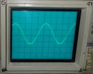
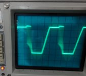
That was the problem. Everything works right now. Sine and Square waves look good. Music sound good. However, it clips ugly. Latches up badly. I am attaching some pics. One is the sine wave just before clipping and the second is at the point of clipping. Both boards do the exact same thing.
Blessings, Terry
Attachments
OK Guys,
That was the problem. Everything works right now. Sine and Square waves look good. Music sound good. However, it clips ugly. Latches up badly. I am attaching some pics. One is the sine wave just before clipping and the second is at the point of clipping. Both boards do the exact same thing.
Blessings, Terry
Hi Terry,
I've had some latching but not so much as you have, I could not find the photos to show.
You can tray to increase R37 to 6k8 or even higher to 10K. It should make clipping better. It's not easy to make VFA with TMC to clip with no latching without Backer clamps, but in this case you have to have separate power supply for IPS with higher voltage then that for OPS.
How about thermal tracking? If it's overcompensated you can increase R35 to next value, and if it's undercompensated you can decrease R30 to next value. I prefer a bit overcompensated.
BR Damir
I had some latching on the Honey Badger. OS came up with a solution but I will have to look back to see what he did. It wasn't nearly as severe as this one. It looks perfect right up to the point where it starts to clip and then it goes ballistic. You can hear it in the boards. I will try increasing R37 and see if that helps. I personally would never play the amp that loud, but if someone did, I can't imagine it being kind to your speakers.
I don't know about the thermal compensation yet because I haven't played it long enough. I only have it mounted to some large angles right now. I need to clamp those to a heatsink so I can let it come to full heat and see what it does.
Terry, I would be interested for two or four pcbs depending on expected price.
That's fine. I will go ahead and order some boards then. It takes about three weeks so we're looking at mid February. PM me and we can work out the costs.
Blessings, Terry
Hi Terry,
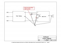
It is very important to do the grounding in a correct way, it can influence a latching too. Here is how I do the ground scheme.
If you want to take the best from TT amp I suggest you to build the PS regulator explained in this thread too, but before you do the PCB check with me for the last layout.
BR Damir
Attachments
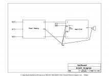
Please, so I can understand, what does R3 do, since you have essentially shorted it by running both sides of it to the star ground?
I've tried to explain it some post back, here http://www.diyaudio.com/forums/solid-state/182554-thermaltrak-tmc-amp-32.html#post4182186, but it looks with no success.
You can tray with no ground connected to the ISP lifted gnd and decide by yourself what you like more.
Hi Damir,
That doesn't really answer my question. I am just trying to understand. If the input ground is connected to star ground and the pwr ground is connected to star ground, does R13 serve any purpose?
Thanks, Terry
Hi Terry,
On the board you are using there three separate grounds, OPS power ground, IPS power ground and IPS signal ground. R3 10R resistor is connected between IPS power ground and IPS signal ground. This resistor some call a ground lifter and some a ground loop breaker. During initial test of the single board I don't connect IPS signal ground to the common ground, but when assembling the amp in to an enclosure I connect all three(or two if ops and ips power ground are not separated on the PCB) to the common star ground and I never had any hum or buzz. Yes you don't need that R3 resistor if you allays connect all ground to the star ground, but it facilitate initial test and does not harm if stays there.
BR Damir
Thanks, that makes sense now. I am still quite concerned about the sever latchup I see on my amp. I did not get a chance to try changing the resistor today. However, I did find where OS had dealt with it in the Honey Badger. It begins with this post. I looked at the Honey Badger schematic and the front end is very similar to this amp aside from the input pair being FET on this and BJT on the HB. I wonder if you think the same diode fix he used on the HB might work on this amp. What do you think?
Thanks, Terry
Thanks, Terry
- Status
- This old topic is closed. If you want to reopen this topic, contact a moderator using the "Report Post" button.
- Home
- Amplifiers
- Solid State
- ThermalTrak+TMC amp