The reason why the LM2941 low dropout regulator IC only manages -75dB rejection at DC, is because its error amplifier has finite gain. What happens instead if you drop in the highest gain opamp natively supplied by LTSPICE, namely, the LTC1150? You get -180dB of rejection at DC, that's what happens. Parts count also goes up, from 5 parts to 10 parts, but maybe you've got the room so it's not a big deal.
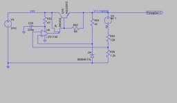
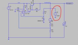
Notice that the large negative pinchoff voltage of the JFET means: no level shifter is required. Also notice that the voltage reference is pretty large: 15V zener, not 6.9V IC. This means we don't throw away precious gain, overcoming the R4-R5 attenuator.
_
Notice that the large negative pinchoff voltage of the JFET means: no level shifter is required. Also notice that the voltage reference is pretty large: 15V zener, not 6.9V IC. This means we don't throw away precious gain, overcoming the R4-R5 attenuator.
_
Attachments
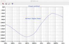
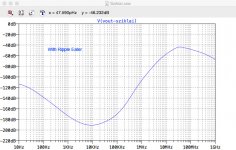
And yet if I drop this circuit into the Sziklai circuit outlined here - after C5 and ahead of the current source - the difference in modelled line rejection is pretty much immaterial... Seems counterintuitive to me.
Attachments
Of course the quantity of interest is the quantity not plotted.
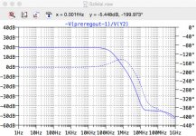
Plotting (V(Node_Y) / V(Node_X)) will show the line rejection of the Sziklai Super Regulator itself
Your plots in #122 suggest that one or the other of them has no line rejection at all, in simulation.
It almost sounds like LTSPICE is using less stringent accuracy requirements (e.g. bigger GMIN, bigger ABSTOL, bigger VNTOL, etc) in your simulations than in mine. Double check this and/or include an explicit directive
- Node_X = output of (LTC1150+MJL3281 ripple filter)
- Node_Y = output of Sziklai Super Regulator
Plotting (V(Node_Y) / V(Node_X)) will show the line rejection of the Sziklai Super Regulator itself
Your plots in #122 suggest that one or the other of them has no line rejection at all, in simulation.
It almost sounds like LTSPICE is using less stringent accuracy requirements (e.g. bigger GMIN, bigger ABSTOL, bigger VNTOL, etc) in your simulations than in mine. Double check this and/or include an explicit directive
- .OPTIONS GMIN=1E-12 ABSTOL=1E-12 VNTOL=1E-6
I found my problem. I had not adjusted your FB voltage divider ratio - or my input voltage - to accommodate the fact that I have two 2.2R resistors in series ahead of the "ripple eater". Voltage input to the ripple eater was too low for its set output voltage.
It looks like it could be a very interesting circuit. It might well be fine to have both pass transistors on the same heat sink. Very compact. (Modelled output impedance is worsened versus straight Sziklai but still rather good.)
(Note that when I inserted a compensation cap from the inverting input to the AD817A op amp in the Sziklai circuit to this op amp's output to provide for a bit more phase and gain margin - well before I looked at your "ripple eater" changes - I needed to use .options gmin=1e-10 abstol=1e-10 to get the .tran analysis to converge properly. But such accuracy requirements weren't the issue here.)
Last edited:
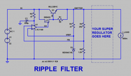
When you're removing ripple by active circuitry, you can save money and board area by not trying to remove it with large electrolytic capacitors and series RCRC filters. Just choose a single C which gives a rippling "raw DC input to regulator" waveform whose lowest voltage ("trough") is still large enough to ensure that everything downstream gets all the voltage it wants. Forget the series Rs, they have a terrible benefit/cost ratio: they drop the voltage by 4.4 volts when 1 amp is flowing, but add only ~10 dB of enhanced line rejection compared to R=0. Far better to spend that 4.4 volts on a cascade of three series LM2941s and get 3x75 dB enhancement of line rejection.
If dBs of simulated line rejection is what you care about most.
Just plunk down enough of your personal favorite electrolytic capacitors in parallel, to get about 10,000 microfarads. With 1 amp flowing that'll give about 1 volt of ripple, Vpeak-1V = Vtrough. Assuming full wave rectifiers and 50 Hz mains.
If dBs of simulated line rejection is what you care about most.
I don't care about simulated except as to inform me of potential/appropriate circuit design. But I guess it begs the question: what makes an excellent voltage regulator? A functioning and stable regulator with:
- Excellent line rejection
- Excellent load rejection
- Low noise
- Low output impedance (as Jack's shootout seemed to indicate)
- Relatively efficient (although in DIY we can afford to squander a bit more wattage)
- Relatively compact (although in this instance we're not trying to design drop-in replacements for 7805 etc)
- Cost effective (reasonable latitude here as we're not doing enormous production runs and hence modest incremental unit cost remains beer money)
At some point the last four place limits on the first three, but there's still a good deal of room for some interesting stuff.
Last edited:
Sure, just double check the .DC run to verify that you're not running the JFET with forward biased gate-source junction, and also to verify that the opamp's output voltage is nowhere near the limit of its output swing. Then run a separate simulation to plot the I-V curves of the various JFETs you've tried, to make sure you haven't accidentally chosen among FETs based on the output conductance of their SPICE models, which are not . entirely . trustworthy to say it diplomatically.
I would have thought the JFET source resistor "R1 68 ohms" might have been the adjustment knob with the greatest impact. But as I often say when confused, the purpose of software simulation is to correct faulty human intuition.
I would have thought the JFET source resistor "R1 68 ohms" might have been the adjustment knob with the greatest impact. But as I often say when confused, the purpose of software simulation is to correct faulty human intuition.
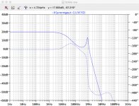
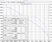
Did you by chance look at the stability of the circuit in post 121? Perhaps I am doing something wrong, but my analysis thus far suggests it is far from having suitable phase and gain margin. In fact, the phase profile is rather peculiar. It doesn't seem easily cured with an output cap/ESR combination either.
No it was a quick and dirty test to find out "what happens when you throw massive gain at the problem?" I figured that the phase shift introduced by the output stage (running at high current!) would be teeny tiny at the unity gain frequency of the opamp. When you use a faster opamp with a higher unity gain frequency (red curve) you do start to see some peaking that looks dangerous.
Maybe it was all too good to be true? Maybe the smart thing to do with a budget of ten parts, is to build two cascaded stages of LM2941s instead of one LTC1150 filter. Let the guys from TI worry about stability as indeed they already have. All you gotta do is guarantee that the net ESR of your bank of output capacitors, is right in the center of their Fig.13 safety zone. Which for my eyeballs is ESR=sqrt(0.1R * 1.0R) = 0.31 ohms. Three big mama capacitors, each one with a 1.0 ohm resistor between cap_minus and GND, boom done.
_
Attachments
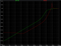
It's not that important to me so I didn't invest huge amounts of time, but I am mildly curious about it. So I invested tiny amounts of time. Instead of breaking the feedback loop and measuring the open loop gain and phase -- which would have taken Real Effort -- I just ran a transient analysis with a fast risetime square wave load. If the thing is definitely, certainly unstable, it will fail badly in a transient test.
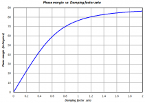
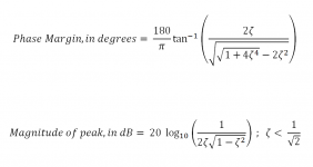
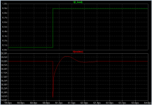
Schematic and simulation results below. When the load current jumps up, from 50mA to 900mA, the output rings a little bit but doesn't oscillate. My best estimate is that this waveform's damping factor is Zeta=0.45 or therabouts. Which corresponds to a phase margin of 46 degrees (figure below). Not disastrous.
When the load current jumps down, from 900mA to 50mA, the output rings slightly more but still doesn't oscillate. My best estimate is that this waveform's damping factor is Zeta=0.38 or so. Which corresponds to a phase margin of 41 degreees. A tad more underdamped but still, not disastrous.
I've copied a couple figures that I originally posted on 18 Aug 2014, showing the relationship between phase margin and damping factor Zeta for a second order linear system.
_
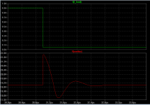
Attachments
Ok. FWIW I've attached a screen grab of what I get when I model phase and gain of that circuit.
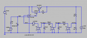
The 'beauty' I saw in a single pass transistor in a pre-reg stage is that this transistor can potentially share the heat sink of the Sziklai regulator stage.
I assume 'bank of output capacitors' is any and all caps sitting on the output of the pre-reg circuit including those biasing the Sziklai regulator stage and its output caps. I'm still having trouble modelling with TI's LM2941 model dropped into the front of my Sziklai circuit. Vout of the LM2941 is correct but the current isn't. It immediately slams into what I presume is the limiter and then drops to zero. So there's nothing to feed Sziklai.
EDIT: our posts crossed. Yes, I too noticed it survived a transient analysis but then I played around a little more. Adding a bypass cap on the op amp supply threw it into haywire. So the circuit as is seems to make it through the transient test by the skin of its chin. And it's got a whole additional regulator circuit to follow it.
The 'beauty' I saw in a single pass transistor in a pre-reg stage is that this transistor can potentially share the heat sink of the Sziklai regulator stage.
All you gotta do is guarantee that the net ESR of your bank of output capacitors, is right in the center of their Fig.13 safety zone. Which for my eyeballs is ESR=sqrt(0.1R * 1.0R) = 0.31 ohms. Three big mama capacitors, each one with a 1.0 ohm resistor between cap_minus and GND, boom done.
I assume 'bank of output capacitors' is any and all caps sitting on the output of the pre-reg circuit including those biasing the Sziklai regulator stage and its output caps. I'm still having trouble modelling with TI's LM2941 model dropped into the front of my Sziklai circuit. Vout of the LM2941 is correct but the current isn't. It immediately slams into what I presume is the limiter and then drops to zero. So there's nothing to feed Sziklai.
EDIT: our posts crossed. Yes, I too noticed it survived a transient analysis but then I played around a little more. Adding a bypass cap on the op amp supply threw it into haywire. So the circuit as is seems to make it through the transient test by the skin of its chin. And it's got a whole additional regulator circuit to follow it.
Attachments
Last edited:
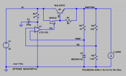
Ok I'm struggling to see the error. I'm breaking the loop ahead of the upper feedback resistor and injecting a small signal AC. Attached are pics of the circuit and output. (The output differs from above as the circuit above inadvertently included an output capacitor I was playing around with.) I've used the 'Linear Tech tutorial method' of breaking the loop. If I break the loop with a 1GH inductor and inject a small signal AC via a 1GF cap immediately after it a la Cordell I get the same answer below 10MHz.
Attachments
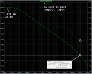
That was an interesting exercise. I took my circuit and modified it to follow yours, checking the output as I went. I shifted the injection point to after the upper feedback resistor, but this made very little impact. (I have been told that it is better to pick the highest impedance point for the injection and this is why I placed it where I had.)
The voltage dependent voltage sources and the fake resistors and caps made no discernible difference and perhaps omitting them can make the analysis easier to perform.
I inverted the AC stimulus as per yours and change the plot from -Output/Input to Output/Input which saved some addition. So far no real change. (Note I had changed your R4 from 252 to 120 to yield a lower output voltage.)
The change of significance was the supply to the Vref Zener which I had left connected to the output and which you shifted to a perfect voltage source. Change that and boom goes the gain! I'm still trying to get my head around why.
Phase margin remained c30 degrees throughout.
I had been modelling none. (I was more focused on the large difference in gain profile.) If I add 900mA of load I get a phase margin of 33.8 degrees using your method (which I can simplify for the same result by removing all the E sources etc) but one difference between your model in post 135 and mine is that I have left the RC filter on the V+ to the LTC1150.
With no load current the NPN transistor is completely off and the JFET supplies the miniscule currents for the feedback divider and for the zener bias. That's why Teddy Pardo connected his JFET source resistor differently: he foresaw that boneheads might run his regulator with negligible load current.
- Status
- This old topic is closed. If you want to reopen this topic, contact a moderator using the "Report Post" button.
- Home
- Amplifiers
- Power Supplies
- Thermal considerations for Fairchild SDIP bridge rectifiers