A variant which leverages earlier experience...and a toggle switch for 115/230V operation. ( Perhaps I should put this in a new thread.)
Pics:
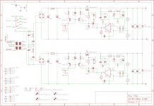
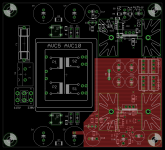
1. Circuit
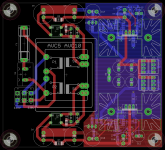
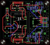
2. Full board (all layers)
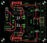
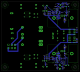
3. Top layer - routing
4. 2nd layer - GND plane
5. 3rd layer - V- plane
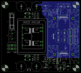
6. Bottom layer - routing
Pics:
1. Circuit
2. Full board (all layers)
3. Top layer - routing
4. 2nd layer - GND plane
5. 3rd layer - V- plane
6. Bottom layer - routing
Attachments
Hi Mark. Bleeders can/will be added. An omission here when importing the design over from my earlier project.
Regarding your second point, I had asked in post 55
Are you suggesting the switch's pin spacing doesn't provide for use in such application or I have done something wrong in implementation? I have trouble rationalising a 120mil rule of thumb against the placement of the central pins on the primary side of the transformer. These are closer together than the switch pins.
PS: I see I have my 115V and 230V labels back to front.
Regarding your second point, I had asked in post 55
It would seem sensible for me to consider in future iterations using an AVC series transformer and incorporating a small switch to allow changing between series and parallel configuration of the primaries.
To that end, I'd like to check if there would be any issues (particularly with respect to safety) of using a small DPDT slide switch such as a Grayhill 48ASDP1S1M2QBT (Mouser link) (Datasheet link) for this purpose. It would seem suitably small and is rated for 250VAC and 5A. I check because mains voltages make me safety conscious.
Are you suggesting the switch's pin spacing doesn't provide for use in such application or I have done something wrong in implementation? I have trouble rationalising a 120mil rule of thumb against the placement of the central pins on the primary side of the transformer. These are closer together than the switch pins.
PS: I see I have my 115V and 230V labels back to front.
Last edited:
I'm recommending that you find someone who knows more about the topic than all of these websites put together
and ask him/her to review your layout. Or, read all those websites yourself and when you are confident you understand them all, then review your layout one more time.
I am not the expert you seek.
and ask him/her to review your layout. Or, read all those websites yourself and when you are confident you understand them all, then review your layout one more time.
I am not the expert you seek.
I've been through tons of similar pages. It's all as clear as mud although the most common guidance is 3mm (just under 120 mil and hence my mention of it above) for European voltages when a protective earth is used (Class 1) and the device isn't subject to extreme conditions/heavy dirt etc. Typical terminal spacing for these mini slide switches is 4.7mm but the solder pads reduce that significantly.
The alternative is (a) a switch designed more for purpose such as a C&K V80212MS02Q (data sheet) with its significantly greater pin pitch and overall size, or (b) abandoning the idea of mains voltage flexibility within the board itself.
I'm open to input from all.
EDIT: actually (a) may well fit with a bit of juggling and is inexpensive
Last edited:
This provides for 120mil/3mm clearance which I understand to be the requirements for Class 1 (safety earthed equipment). I will have to get hold of an actual switch part to confirm I have the connections around the right way (i.e. that when 230V is displayed I do indeed have the transformer connected for 230V operation and not 115V).
I think the reason why transformer pins 4 and 3 can be closer together is because with 230V operation they are connected while in 115V operation, when they're not connected, the required clearance is lower. In any event, I had oversized the pads and I have now reduced them which increases clearance.
AndrewT, this topic is normally right down your alley, no?
Attachments
Last edited:
Hi SGK,
I would recommend to move the red trace (top layer?) which goes from C18 to the via next to D12 such that it does not go under the heat sink. If solder mask and anodizing get scratched you may create a short there. Also I think you do not need paralleled output caps (C19,C21 and C20,C22). A single capacitor per rail should be sufficient, IMHO.
Regards,
Oleg
Note to Mark - I will add the bleeders...
@OlegSH. Re trace good idea given easily managed. I always use washers under heatsinks but here this can easily be changed. Re the output caps, more is better but more importantly this circuit has been thoroughly transient/stability tested with the two caps so I won't be changing this.
@OlegSH. Re trace good idea given easily managed. I always use washers under heatsinks but here this can easily be changed. Re the output caps, more is better but more importantly this circuit has been thoroughly transient/stability tested with the two caps so I won't be changing this.
@OlegSH here is a link to prior transient/stability testing of this circuit. I guess decreasing load capacitance at the regulator output would move the output pole to a higher frequency increasing phase margin. But reducing capacitance also reduces ability to supply transients. Given it is tested as configured and a cap costs very little, I'll leave it where it is.
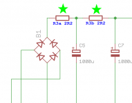
If you split R3 into two series pieces, each 2.2 ohms*, and put half of it before the very first filter capacitor C5, two good things would happen. First, you'd get more ripple filtering. Second, the tall and narrow current pulses which charge the filter capacitors, would become shorter and wider. Less stress on your transformer, less peak current through your diodes, less dI/dt to emit RFI, less L*dI/dt to stimulate ringing of the secondary. The current pulses would have the same area as before (Q = integral(Idt)) because you're delivering the same charge-per-AC-mains-cycle to the load. But short wide pulses are less awful than tall narrow pulses. And it costs approx. nothing: two resistors.
You could also consider changing C3 and C4 to 1uF which is not costly: Mouser link. Now you can overdamp the secondary at zeta=2.0 if you wish, and get smooth, smoooooth waveshapes on your Quasimodo.
*Or, 1.8R and 3.0R if you prefer
_
You could also consider changing C3 and C4 to 1uF which is not costly: Mouser link. Now you can overdamp the secondary at zeta=2.0 if you wish, and get smooth, smoooooth waveshapes on your Quasimodo.
*Or, 1.8R and 3.0R if you prefer
_
Attachments
Last edited:
@OlegSH here is a link to prior transient/stability testing of this circuit. I guess decreasing load capacitance at the regulator output would move the output pole to a higher frequency increasing phase margin. But reducing capacitance also reduces ability to supply transients. Given it is tested as configured and a cap costs very little, I'll leave it where it is.
AFAIK, paralleling capacitors can be used for two reasons: to increase capacitance and to reduce ESR. Both of which can be achieved by using one bigger capacitor which will have proportionally lower ESR. From the point of view of components count you are right, capacitors aren't expensive. But I guess the biggest problem in supplying transients or ensuring stability will be the inductance which is not addressed in your layout if looking at the placement of the capacitors: they are neither close to the pass transistors nor they are close to the point of load.
I am by no means an expert and can easily be wrong here, so may be some one more knowledgeable could comment on this.
Regards,
Oleg
they are neither close to the pass transistors nor they are close to the point of load.
I am by no means an expert and can easily be wrong here, so may be some one more knowledgeable could comment on this.
Regards,
Oleg
My ears are open
")
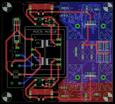
I will rotate C19 into the pocket at the back of the heat sink to shorten the V+ trace to the output connectors.
C20 and C22 are kind of weird. GND is a plane on the right side of the board because of the multitude of touch points. V- is also (although I used a trace to connect the input to the feedback network on the V- side to the output connectors rather than tapping the V- plane). So at the moment C20 and C22 only have planes connecting them...
This pic shows what I mean. I have turned off the GND and V- planes. It kind of emphasises Oleg's point regarding the placement of output capacitance. But then again, (I think) the V- plane does represent the lowest impedance path to the output connectors.
Attachments
Last edited:
I think it depends on what the output capacitance is expected to do.
Does the output capacitance provide a load that the active stage requires to remain stable? In which case the capacitance should be located to best perform that duty.
or
Does the output capacitance lower the output impedance that will be seen by the variable load? In which case the intervening cables ruin any hope of maintaining that low impedance and the capacitance should be located at the load where it can be placed to maintain a low source impedance, if that is what the load requires.
or
The capacitance must do both jobs !
Locate it to stabilise the active stage AND locate it at the load where it can provide a low source impedance for the load.
This pic shows what I mean. I have turned off the GND and V- planes. It kind of emphasises Oleg's point regarding the placement of output capacitance. But then again, (I think) the V- plane does represent the lowest impedance path to the output connectors.
To confuse you even more...
I remember reading somewhere on this forum, that if you lay a trace over the wide plane you effectively put most of the stray inductance in series with that trace. As the result the largest transient will be seen on that trace. In your case the lowest transients will be seen on the V- of the positive side (you call it GND) and on the V- of the negative side because that's where you use planes if I understood your layout correctly. But the lowest transient of the negative side should probably be on its V+ since it connects to a common GND point for pos/neg legs of the regulator. Thus the V+ of the negative side should have lowest inductance, e.g. be a plane. The layout can be simplified if you take a similar arrangement as in Jung/Didden superreg where the positive and negative sides are symmetric using complimentary pass transistors. This would allow you to use one common GND plane everywhere. Or you can drop the on-board GND connection all together and connect the pos/neg sides together at the load... as Jan Didden did on his boards.
All above is IMHO...
Oleg
In your case the lowest transients will be seen on the V- of the positive side (you call it GND) and on the V- of the negative side because that's where you use planes if I understood your layout correctly. But the lowest transient of the negative side should probably be on its V+ since it connects to a common GND point for pos/neg legs of the regulator. Thus the V+ of the negative side should have lowest inductance, e.g. be a plane.
V+ of the negative side is the plane I call 'GND'. (Layer 2)
V- of the negative side is the plane 'V-'. (Layer 15)
Only V+ of the positive side isn't a 1/2 board plane from pass transistor output to connectors although I have used a smaller plane with a view to lowering the impedance between such.
The layout can be simplified if you take a similar arrangement as in Jung/Didden superreg where the positive and negative sides are symmetric using complimentary pass transistors. This would allow you to use one common GND plane everywhere.
But that would defeat the purpose of using this MOSFER pass transistor design with its higher current capability (the Jung/Didden reg caps out at around 100mA if I recall correctly) and potentially better line rejection.
Here there is just one GDN plane also. I merely segregate the right side of the board from the left side which is subject to rectifier pulses (and there's no need to take it to the bottom of the board). The only 'quirk' is that V- (low side of negative regulator) is also a plane rather than a trace given the vagaries of using a +ve regulator to generate V-.
The circuit you see here (well, in it's single +ve regulator form) was developed to be 5A+ capable for another project. (See previous links.) It was developed with enormous help from Mark Johnson. I deviated from Mark's guidance when I decided to power the op amps and Vref from Vout as with the Jung/Didden regulator at Jan's suggestion. Mark has posted in more detail re his version of the circuit in this thread here. The more I think about the idea of powering Vref and the op amps from Vin rather than Vout to achieve better load regulation the more I find it compelling, but I'm sticking with this simpler circuit for now.
So...I'm merely pointing out the 'quirk' that because V- is a plane the two output caps on the V- side couple planes rather than a trace and a GND/0V plane. It just kind of looks a bit weird.
EDIT: having just enlarged the polygon from +Vreg out to the output caps and connectors it becomes more obvious that this is just a visual quirk. The greater I enlarge the V+ out plane the more analogous it is to the V-.
Last edited:
Now I understood the entire layer structure! It seems that the only "asymmetry" in the PCB layout is the V+ of the positive side. Since the top layer is almost empty and you plan to use spacers under the heat sinks nothing prevents you from making a copper pour for the positive side V+ .
I recall that you had trouble before when you used the IDSS of a MMBF5460 as your current reference. Datasheet says: 1mA to 5mA but LTSPICE model disagrees. LTSPICE model is wrong-ola.
I recommend you switch to MMBFJ108 or PMBFJ109 + source resistor. I have a dozen of each, in thru hole, and can do a quick protoboard measurement to find the right resistor value that gives the current you want. Just tell me (a) which NJFET you will use; (b) what current you want. I'll figure out the right resistor value.
Then, as before, you can verify that you're getting ZACKLY the current you want in your final product, by measuring the voltage across R5 (post#61) with a digital voltmeter. Ohm's Law tells you the current.
- Status
- This old topic is closed. If you want to reopen this topic, contact a moderator using the "Report Post" button.
- Home
- Amplifiers
- Power Supplies
- Thermal considerations for Fairchild SDIP bridge rectifiers