well the OP started with a design based partly on marketing speak ie minimal parts gain clone. He was then directed to NS data sheets where an engineer still needs to be able to read between the lines to seperate the wheat from the chaff so to speak [...]
As I posted earlier I'm still trying to get the hang of all the parts and I think the "maximum" configuration is not that bad a start since I can build the amp, omitting these parts and have a direct comparison.
so the only parts that are missing from "maximum" are Ci and Rf2/Cf which act as RF-filters, but thats true for every part I guess... To ask a totally ignorant question (since I really have no imagination what they are for) is it useful to include these?
cheers!
beginners and those with less experience in debugging faulty assemblies are advised to always use all components that improve the chances of avoiding instabilities.
With experience one can try omitting some of these components when one knows what to examine to determine that this "cut-down" version is indeed stable with all audio signal and all audio loadings.
With experience one can try omitting some of these components when one knows what to examine to determine that this "cut-down" version is indeed stable with all audio signal and all audio loadings.
Then I only have one quick question left, what should be the value of Ci? I only have access to the Wima MKS-2 up to 6.8uF and the datasheet says, it should be 10uF and not an electrolytic. So a question for the experts which value would be ok for this.
(well actually also 10uF but only ~17mm grid).
Thanks and cheers!
(well actually also 10uF but only ~17mm grid).
Thanks and cheers!
Thanks for the quick reply, now with "maximum" parts, since my Rg is 22k 4.7uF is the cap of choice.
L is now wound around R, 13 to 14 turns should give an inductance a bit above 0.5uH
Added diamond pads for pin 2 & 6.
Size: 30 * 40mm
New parts are:
AMP: v5.0
Hmm I've got at least 15mm² in the top left corner left over")
cheers!
L is now wound around R, 13 to 14 turns should give an inductance a bit above 0.5uH
Added diamond pads for pin 2 & 6.
Size: 30 * 40mm
New parts are:
Code:
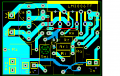
Rf1: 22k
Cf: 50pF
Ci: 4.7uF
AMP: v5.0
An externally hosted image should be here but it was not working when we last tested it.
Hmm I've got at least 15mm² in the top left corner left over
cheers!
Some basic information on how signals travel round a PCB that you may find useful. Personaly I think some have a tendency to overcomplicate the ground structure of some of these small designs, especialy when you take EMC into consideration, but as home designs very rarely get tested for EMC you dont get the same feedback as when these types of chip amps are used in other designs (commercial, millirtary etc). Anyway this sis a simeasy to understand guide on how the signals travel around the pcb etc:
http://www.x2y.com/filters/TechDay0...log_Designs_Demand_GoodPCBLayouts _JohnWu.pdf
What you need to do is start thinking interms of waves not electrons traveling around as electrons are lazy little ********** and only move at about 8.4cm per hour
http://www.x2y.com/filters/TechDay0...log_Designs_Demand_GoodPCBLayouts _JohnWu.pdf
What you need to do is start thinking interms of waves not electrons traveling around as electrons are lazy little ********** and only move at about 8.4cm per hour
Thanks for the link marce, I've looked through it and the diagram for the current flow on double sided PCB's was very interesting. But most of it is just a league to high for me (for now )
I hope that the size of my PCB will make up for the imperfections in wiring but now with star-grounding I don't think there's too much left to do better, considering the size.
cheers!
)I hope that the size of my PCB will make up for the imperfections in wiring but now with star-grounding I don't think there's too much left to do better, considering the size.
cheers!
Tried to edit my post, but stupid 30 min rule so i deleted it again and here is the edited version: Re schematic, i drew it myself. looks good.
Further, i would have just simply connected the ground leg of Rg to in-. (smaller ground loop)
Holes of Rf can be small size, move Cf down, and connect Rf to that trace spot.
connect Cf to the branch Rf was connected to.
Further, i would have just simply connected the ground leg of Rg to in-. (smaller ground loop)
Holes of Rf can be small size, move Cf down, and connect Rf to that trace spot.
connect Cf to the branch Rf was connected to.
Last edited:
OK, i had a look at the datasheet of lm4780. place Rin after Rb. This is better for DC offset. (both in+ and in- should have same impedance to ground)
The polarity of Cs1 is wrong.
fyi ive built this amp but without the (Rf + Cf)//Rfi because i only use a gain of 11 anyway. The purpose of this network is to bring the gain down to 10 for high AC freq. Dont go below 10 as it will oscilate.
i get 3.4mv dc offset input shorted. This is very good. The way to do this is match Ri and Rb, and Rg to Rf. ( same story as above, in+ and in- should have same impedance to gnd.)
Last edited:
excuse my comment "Further, i would have just simply connected the ground leg of Rg to in-. (smaller ground loop)".
Better is to seperate the power gnd star from the signal gnd star. Easiest way to do this is make the GND of Ci cap the signal gnd star, so just connect In- and Rg- to that point
Better is to seperate the power gnd star from the signal gnd star. Easiest way to do this is make the GND of Ci cap the signal gnd star, so just connect In- and Rg- to that point
Last edited:
fyi ive built this amp but without the (Rf + Cf)//Rfi because i only use a gain of 11 anyway. The purpose of this network is to bring the gain down to 10 for high AC freq. Dont go below 10 as it will oscilate.
Ok, I see, thanks for translation datsheet <-> human
!The polarity of Cs1 is wrong.
Better is to seperate the power gnd star from the signal gnd star. Easiest way to do this is make the GND of Ci cap the signal gnd star, so just connect In- and Rg- to that point
You mean like this?
Holes of Rf can be small size, move Cf down, and connect Rf to that trace spot.
connect Cf to the branch Rf was connected to.
This I don't quite get, you are saying, that the upper pin of Cf should be closer to Cz, and the left pin of Rf behind Cz?
Because this is one of the few possible arrangements of Rf/Rf1/Cf.
Thanks for your explanations btw!
AMP: v5.1
An externally hosted image should be here but it was not working when we last tested it.
cheers!
P.s. Please ignore the thin yellow connection between Cz and the jumper-island.
Last edited:
I mean like in the attatchment below. I realize i wasnt clear enough, sorry.
Not sure if Cf will fit like that. It might take some fidling around. Probably rotating a bit to the left and moving RnL lower will work.
Also, let traces cross at right angles.
Additionally add a C of ~15pf directly at the signal input (p22 fig 7 of lm4780 datasheet).
Not sure if Cf will fit like that. It might take some fidling around. Probably rotating a bit to the left and moving RnL lower will work.
Also, let traces cross at right angles.
Additionally add a C of ~15pf directly at the signal input (p22 fig 7 of lm4780 datasheet).
Attachments
Ok, I've included your suggestions.
AMP: v5.2
cheers!
Is this a rule of esthetics or electricity?Also, let traces cross at right angles.
AMP: v5.2
An externally hosted image should be here but it was not working when we last tested it.
cheers!
Ok, I've included your suggestions.
Is this a rule of esthetics or electricity?
Its to not have inductive coupling.
I think its starting to look pretty good now.
Few more places i would let paths cross at 90 degrees are the Rm and jumper, RnL and the ground trace below it.
The signal input traces can be a little smaller. The spacing is tight over there, and they dont carry current anyway.
Make the GND star more of a star. Look at p23 of lm4780.
Can you make the Vn, Vp, and Out traces fatter?
Check, increased the power traces from 2mm to 2.5mm. (where possible)
AMP: v5.3
AMP: v5.3
An externally hosted image should be here but it was not working when we last tested it.
You can keep the copper pad enclosing the two Gnd points. Saves etching solution. Also make a circle in the cross of the signal gnd. Make Out- fatter, and the path RnL to the chip pin.
Move Cz down so you can make more clearance with the jumper island.
Can the Rb to Rg trace be made a tiny bit thinner?
whats the board area now?
Move Cz down so you can make more clearance with the jumper island.
Can the Rb to Rg trace be made a tiny bit thinner?
whats the board area now?
Last edited:
Rb to Rg from 1.1 to 0.9mm.
Out-/+ now 2.5mm
RnL to Chip 2mm
Board is exactly 40 * 30mm
AMP: v5.4
edit:
Out-/+ now 2.5mm
RnL to Chip 2mm
Board is exactly 40 * 30mm
AMP: v5.4
An externally hosted image should be here but it was not working when we last tested it.
edit:
Too late ;-) looks fancier now anyway.You can keep the copper pad enclosing the two Gnd points.
Last edited:
- Status
- This old topic is closed. If you want to reopen this topic, contact a moderator using the "Report Post" button.
- Home
- Amplifiers
- Chip Amps
- The yet tiniest single-sided LM3886?