wow... 3 postings, while I was preparing one...
...
") change.."AC97" on system..please.
change.."AC97" on system..please.ok ,I agree with you even on "DT" .
signal is not clean, also up-side drivers not Have RC filter (constant) on bootstrapp. (it modulate)
perhaps the effects are positive, we can not evaluate these images only.
and then I see a lot of ripple on the power supply at ...only 500w?
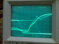
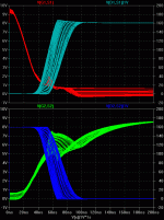
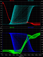
The shades in the pictures represent a family of traces for all possible output currents during one cycle of sine wave. A single image tells how the circuit behaves at many different current levels. A smooth shade tells that the waveform is changing smoothly and without discontinuities as output current is increased.
Dead time results in discontinuities and hot spots in the shade becauase it makes the delay (and the traces) jump.
Please capture and show us your waveforms to demonstrate that you know what you are talking about. Not everybody knows how to capture these waveforms at 20ns/div. Once you learn to capture them, next step is to learn to interpret them and use the information to fine tune the circuit.
Essentially, the goal is a smooth shade that grows linearly with input signal, which is more or less what I get.
Last edited:
Eva:
...well, now starting to wonder.
Your screen shoots do show shades on Uds and Ugs as well.
If triggering to Uds, then I would expect a more or less stable Uds shape and shades for Ugs only....
What is giving your trigger signal?
Comparator output, the only true reference
The variable delay from comparator output transitions to switching node transitions is a strong source of non-linearity (a more general way to analyze dead time distortion), so it's something worth fine tuning.
Last edited:
this is my new job on a modulator with integrated driver (up to 4 independent MOSFET) and includes a system of exchange DT realtime.
yes ... I work with very little time (see 10 nS).
I like to see the signals (obtain) very clean.
This new PWM for High power modular system (10Kw at cabinet for services)
yes ... I work with very little time (see 10 nS).
I like to see the signals (obtain) very clean.
This new PWM for High power modular system (10Kw at cabinet for services)
Attachments
working with realtime DT changed is possible at digital stage only (not at power stage) it is very poor.
...yup.
As you say. You have chosen the nice looking wave forms.
But we cannot see the relation of Ugs to Uds and also not the influence of various situations.
The only thing we see, is that your modulator has asymetric dead times.
Is this a load adaptive dead time?
...yup.
As you say. You have chosen the nice looking wave forms.
But we cannot see the relation of Ugs to Uds and also not the influence of various situations.
The only thing we see, is that your modulator has asymetric dead times.
Is this a load adaptive dead time?
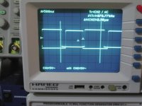
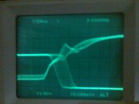
I understand that these signs do not say anything. as soon as possible put also the signals of the MOSFET gate but I can assure you that all this takes place with clean signals. square waves, I care a lot (this applies to all products that I did).
yes, at this time were very asymmetric because I move one side of the PWM, this can not listen when distortion occurs. (This DT changed at F0 / 2) (yes one-one not).
Controll digital circuit operated at pre driver stage, so I provide clean signals to the pair of MOSFETs (direct drive). I have already created a similar system and did not perceive any defect when he plays.
looks like a normal hi-fi amplifier .. but mosfet still cool
Last edited:
tons of guesses...
AP2:
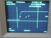
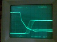
Your PWM-Signal is looking like you measured the signal for the upper MosFet not right behind the modulator, but already behind the level shifter and before the gate drivers by using a differential probe. Correct?
(Guessing this because of the small step in the signal. Step due to limited HF common mode rejection of differential probe?..)
The half bridge jumping up, right when the lower Fet is being turned OFF. Right at the beginning of the dead time. Combined with the modulation index, which seems to show the situation of a positive output voltage..
Together it would indicate very small or no load current during the shown measurement.
...with the modulation index indicating a positive output voltage....
The transition from low side MosFet to high side MosFet would be have a shorter dead time, during positive output voltages...
Means avoiding or minimizing the dead time for hard switching situation when driving a resistive load, while the transition towards the negative direction would happen by the inductor current anyway immediately after turning of. ... and vice versa for negative output voltages...
Correct?
Eva:
Agreed. Using the comparator signal for triggering is adding the information about the delay behavior in the same screen shot. ... you love to see as much effects as possible in one picture... Cool system for seeing immediately whats going on, but difficult for educating others.
AP2:
Your PWM-Signal is looking like you measured the signal for the upper MosFet not right behind the modulator, but already behind the level shifter and before the gate drivers by using a differential probe. Correct?
(Guessing this because of the small step in the signal. Step due to limited HF common mode rejection of differential probe?..)
The half bridge jumping up, right when the lower Fet is being turned OFF. Right at the beginning of the dead time. Combined with the modulation index, which seems to show the situation of a positive output voltage..
Together it would indicate very small or no load current during the shown measurement.
...with the modulation index indicating a positive output voltage....
The transition from low side MosFet to high side MosFet would be have a shorter dead time, during positive output voltages...
Means avoiding or minimizing the dead time for hard switching situation when driving a resistive load, while the transition towards the negative direction would happen by the inductor current anyway immediately after turning of. ... and vice versa for negative output voltages...
Correct?
Eva:
Agreed. Using the comparator signal for triggering is adding the information about the delay behavior in the same screen shot. ... you love to see as much effects as possible in one picture... Cool system for seeing immediately whats going on, but difficult for educating others.
To EVA
I did a critique of the signal EVA Because I believe that can interpret what they read.
why you think I do not understand it well?
I admire you for your knowledge, I probably have more technology, but this means nothing if I can not "read" well what I see.
ok,pwm signal show in IDLE (no signal at input) this save energy, a small input signal switch DT at normally (45nS) sym. after it is controlled by voltage (no current output) but one threshold on current force also DT. this is concept on this new modulator. soon you'll see 4 signals simultaneously on the oscilloscope.
"Deadtime" is still required in order to get the Vgs intercept at roughly Vth. However, Vth obviously varies with a number of factors and is considered poorly controlled, thus would be the deadtime that relies on it. This is poor control for an amp of that power level, especially full bridge, and why you're only showing it at 500W? You'd more accurately call this "variable deadtime", for marketing.
You won't show the THD vs Power at ~7khz, will you? This is bush league.
"he delay from PWM signal transition to switching node transition is determined by output current and is quite linear with respect to output current."
Linearly variable.
"Not matched or selected".... if you didn't select them, how did they find their way in there, volunteer?
The ghosting in your analog scope tells the real story.
"di/dt is regulated to allow reliable use of body diodes with 2R loads (up to 40A per IRFB4227)."
Oh so it's not all thanks to the wonder mosfet like you were originally saying. Does that also helps with the inevitable shoot through?
Looks like you're the guru now AP2.
Actually the inverse of dead time is required to get Vgs intercept right. This rules out most chips with built in dead time, like IRS2092. Some overlap is what the actual circuits ask for. Chocoholic noticed the same phenomena. I assume you have never dealt with the subject in practice.
This happens because the gate has to be charged slower than it's discharged to keep turn on di/dt << turn-off di/dt (the reason for this is mentioned later). In practice, discharging the gate by "shorting" it to the source and relying in internal gate resistance (about 2.2R for IRFB4227) is the best option, as it results in the fastest turn-off for a given transistor. Improving this would require negative bias.
There is no variable dead time at all in my waveforms or my circuits. The variable delay involved by the shades is inhetent to MOSFET (and IGBT) switching. All gate controlled devices turn on at a certain di/dt rate (about 750A/us in my circuit), and drain voltage does not start to fall until drain current has exceeded inductor current plus reverse recovery current, if any. The process of growing drain current to the required value takes a variable amount of time, as inductor current is directly related to input signal.
di/dt control for reliable operation of IRFB4227 up to 40A is achieved through gate drive only. There are no extra parts like diodes or inductors in the current path. Clever use of source lead parasitic inductance and some zeners are the key. In fact, Chinese are going to have a really hard time copying this amplifier, it looks simple by construction, but parasitics (often going unnoticed) are used for advantage in many places.
This di/dt phase results in increasing delay for higher output currents. The relationship is not necessarily linear, it's the job of the designer to linearize it. Sorry but you speak as a simplified text book, as if you had never seen these elementary switching phenomena on oscilloscope.
Shoot through does not happen as long as there is no effective overlap and provided that turn-on di/dt is substantially lower than turn-off di/dt. These slopes are, again, gate controlled without parts in the current path.
I can show gate and drain waveforms at 5000W/2R, but they are essentially the same as for 1500W/4R, the only difference is a 2 to 3 times longer di/dt phase. And of course, they are harder to capture because neither the amplifier nor the electrical system of my lab or my dummy load can handle that power for a long time. It has to be tested in burst mode.
The IR2110 and the IRFB4227 are picked randomly, they are not selected to match certain specs. That's what I was trying to point out. Gate threshold voltage changes very little in the operating temperature range, 10A Vgs is 6.2V at 25ºC and 5.8V at 125ºC, this has negligible impact over switching times, and even over my di/dt control scheme. Everybody knows that MOSFET switching times are not temperature dependent. Why are you claiming the opposite in a desperate attempt to embarrass me?
Finally, I don't have 7khz THD figures, but 4Khz THD is below 0.05% up to -3dB (1500W/4R) and below 0.1% up to -1dB. All this at 240Khz switching. There is also a more efficient subwoofer version switching at half the frequency and flat to 10khz, but with the same PCBs and power stage.
BTW: To the moment, Chocoholic and me are the only ones daring to show switching waveforms in detail, like 20ns/div. My purpose is not to sell anything, this project was already sold before it started and is in production now, what I want is to sort out misconceptions about how things work, and to bring back to the floor the feet of people claiming unsurprising performance to be surprising.
Last edited:
I do not know your work frequency yet, Power Electronics theory is important,I have read a thounds of time.I know in car subwoofer amp use ucd topology like Eva said.
Two way make mosfet cool in half bridge:
1.Enough mosfet drive energy provided
2.Perfect dt time .
I know some company use phase shift technology in full bridge power solution(like intersil),maybe this technology can stop Dt time debate.
Crown BCA technology have not use ,maybe we have to lead to this point.
Please paste some schematic and provide idea good or wrong.
The switching frequencies of the two versions of the amplifier are mentioned on post 33. I think you have trouble both reading and writing english. I'm revealing a lot of information for anyone able to read between the lines. This is a commercial project, I can't just post schematics, my customer is already angry at times because I tell how I make things work.
Last edited:
These pictures are taken at 75W/4R with intentionally added dead time as the previous ones. The dead band grows very fast as output current is increased at first, then it suddenly starts to grow much slower. This transition happens around 75W/4R in my circuit, and it's a major source of non linearity (high order harmonics).
Attachments
Last edited:
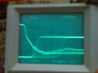
These other pictures are taken at 75W/4R but with no dead time (normal circuit). Now the shade grows more or less proportionally to output current. This is what I call "no dead time", as the non-linearity from dead time is mostly removed. I like the timing consistency between IR2110 samples, and across the temperature range, it allows to work with no dead time in a very reliable way.
Attachments
 Personal snipes and collateral damage deleted. Return to the topic. Discuss ideas, not each other. You all know the rules.
FORUM RULES
Yellow cards given.
Baldin recently made a request in another thread for an LTspice model of a UcD type amplifier with variable dead time so that he might study how it influenced the THD of the audio output. His request intrigued me, so today I made up a reasonably accurate, but still fast running model for LTspice. Not only does it have a comparator-driver section with variable delay time, rise time, dead time and output drive levels (voltage and current), but it also has a fully discrete element power stage that includes most of the important inductances.
Once that was working, I couldn't resist trying to match the waveform photos Eva posted. This required some intelligent guessing of the form of her secret di/dt control circuit. Attached are waveforms for moderate output power with and without added dead time. What do you think? Is it a good match?
Once that was working, I couldn't resist trying to match the waveform photos Eva posted. This required some intelligent guessing of the form of her secret di/dt control circuit. Attached are waveforms for moderate output power with and without added dead time. What do you think? Is it a good match?
Attachments
Hi all,
The figures are good for the sym.
As I mentioned before (in my case) my circuit operates only at pre-driver stage.
I not use chip-driver and the MOSFET directly mate with only the Rg 1R.
I only changed from 30ns to 150ns Dt, this circuit does not intend to reduce the current (some slightly decreases) this removes the bias current so as not to dissipate the power MOSFET (4) Because VD is + /-95V.
to reduce the current power, use another system that does not cause audible distortion. This consists in interrupting either the two pwm (it's simple ... if you can think of). differential current sensing put in a pwm (sync with first) result is PWM (voltage to time) to interrupted up-side / low side signals.
as soon as I have time, put the waveforms of this, so answer the challenge from EVA .. (only two have published measurements with 20ns)
- Status
- This old topic is closed. If you want to reopen this topic, contact a moderator using the "Report Post" button.
- Home
- Amplifiers
- Class D
- The simple way to improve the IRS2092 amp performance