
Hello colleagues . I propose to discuss another scheme . Prototype phase inverter output stage served Van Skoyoka only replaced by cathode followers of the source . The output stage has a unique set of characteristics. it
- Broadband ( Miller grounded through low impedance source follower , the band turns to using a common grid )
- High identity ( balance ) by AFC shoulders , PFC and Rout
- High gain shoulder ( to the transistor m against m / 2 at diffkaskada )
- Good reaction coefficient voltage (PSSR) - low output impedance ( in the cathode circuit no OOS due to the rather large Rout cathode follower )
- Degree of convenience - input circuit between VC and lamp Low-impedance, which allows her not escape , and repeaters be wired directly to the input connector . The driver can shake asymmetrically grounding one of the inputs . Kg with almost no increase ( current of the second transistor flows through "passive" transistor and generates pre-emphasis , which are destroyed , when added to the distortions of the "active" ) Transistors repeaters operate on a large quiescent current and small distortion . Due to the low output impedance of transistor output resistance of the tube is not significantly increased as compared with the passport , and therefore does not gubitsya band .
Netting also working on repeaters and Miller grounded through them. Band close to the band with a common grid.
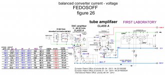
Figure 21 shows a push-pull output interconnections . Due to cross-linking the gain of the output stage is increased exactly twice than the conventional scheme . Furthermore , the output stage becomes a differential signal amplifier . At the same time exactly twice stronger suppressed phase signal - digital noise and noise and power supply. The differential signal is simultaneously applied to the grid and cathode lamp. Space charge grid - cathode becomes adder differential signal . Lamps in this case become a differential signal amplifier . Transfer current from the anode to the cathode, the output tube , and then in the source of driver stage generates current feedback , which also increases the linearity of the output stage and expands Frequency band . Push-pull output crosslinked allows powerful driver transistors IRF9240 " disperse " GM70 and GM80 lamp directly signal PCM1794A, without using additional amplifiers voltage . Furthermore powerful drivers allow the use modes in the output stage A, A1 , A2. That is the mode of the lamp with grid currents . Powerful drivers effectively charge - discharge the structural capacity of the output tubes . Denominations details on the scheme and modes " sharpened " under the powerful modulator tubes GM70 . The amplifier is possible to use almost any output tubes from 6P3S to GU80 .
Attachments
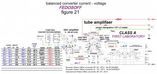
In the diagram on the left side , there is a table with which it is possible to choose the lamp mode independently. From the practice - when calculating modes should proceed from the following . РСM1794A - include in MONO . For AC output voltage V 1 requires 215- ohm resistor . Choose, for a specific lamp , anode voltage, grid bias , the magnitude of the AC voltage applied to the grid lamps and P2 respectively trimmer set the desired quiescent current . The bias voltage is determined by resistors R5 and R19, and the cathode current . Resistors R5 and R19 are set at 20 - 30 % less than the standard of the output stage circuit and the current balance circuit will compensate for these percentages . PP amplifier advantage of the 21st century is that the input of the output stage is fed precisely balanced differential signal High level directly from the DAC chip ( РСM1794A ) . This eliminates interconnect connectors , operational amplifiers directly to CD or DVD device , eliminates unnecessary amplification stages , and also the most difficult stage is implemented - analog phase inverter. In addition, eliminating multiple conversion current - voltage operational amplifiers and a final amplifier .
Last edited:
DAC chip PCM1794A directly integrated into the power amplifier. Switched to mono , for greater impact and to improve the current linearity. PCM1794A sets regimes AC and DC for the entire amplifier is stable currents and temperature changes. Accordingly saved all operating modes of the amplifier with long-term use . With the digital zero , the current flowing from RSM1794A is 13 mA. DR1 and Ap2 inductors included in the collector circuit of transistors T1 and T2 , as well as capacitors C1 , C2 , C3 are applied to suppress digital noise. In the emitters of transistors T1, T2 directly from the DAC chip PCM1794A served arising variable (sound) current ( + - 5 mA at 0 dB). The effluent from the alternating current collectors of transistors T1 , T2 , it is a current DAC chip PCM1794A , creates an alternating voltage audio R1 and the resistor R3. AC voltage level determined by resistors R1 and R3. The level of the AC output voltage is determined by the resistor R1 . In place of the resistor R1 can install stair level control . In place of a single volume control scheme can be set frequency-dependent volume control or combined passive node volume and tone adjustments . Adjusting the volume at the same time - analog , digital and robot over SPDIF. Digital volume is set to maximum. Robot regulated analogue .
In the push-pull output stages of the level determined by the precision harmonic currents in the windings and the magnitude of the AC voltage on the primary windings of the transformer sound . Balance alternating voltage is set by trimmer P3. Current balance is maintained machine. Current balance in the output stage is achieved by changing the negative grid voltage . Current of each lamp is individually and automatically . Scheme current setting for each lamp comprises an operational amplifier and a bipolar transistor , and a measuring resistor . Measuring resistance is included in the drain of the FET , and in fact the cathode lamp circuit . The accuracy of the selection of pairs of measuring resistances accuracy depends balance of current in the primary winding of the transformer. In operation, the amplifier automatically balancing scheme compares the reference voltage and the voltage taken from the measuring resistor and adjusting the grid potential. Current balance scheme operates as follows. Assume that the current of the lamp L1 is bigger now. Voltage at the measuring resistance becomes larger than the reference . Voltage at the output of the comparator will increase the current through the transistor T6 also increase. This will increase the voltage drop across the resistor R12. As a result, the negative voltage on the grid lamps L1 becomes longer , thus reducing the load current . Current balance is restored. The advantage of the proposed scheme - easy , no capacitors in the cathode lamp circuit , automatic balance adjustment current balance adjustment alternating voltage in the primary winding of the transformer. Receipt of any large-scale conversion factor . Reduced intermodulation distortion by eliminating unnecessary amplification stages . The absence of feedback , dynamic distortion , phase shift , coupling capacitors and connectors interconnect . Substantial suppression of harmonics in the output transformer by the precise balance of current and voltage . In the absence of coupling capacitors , the band in the direction of lower frequencies expanded and depends only on the size of the transformer. Current feedback improves the linearity of the output stage and expands bandwidth Frequency . Grid circuit of the output tubes work with small bias resistors R12 and R 13 , which increases the reliability of the tube stage . The gain of the output stage is increased exactly twice . Twice suppressed phase signal - digital noise and noise and power supply. Parameters remain stable long-term operation . Eliminates multiple transform current - voltage operational amplifiers and a final amplifier . The amplifier has the shortest path in the world. Hence the most correct ( reliable ) sound. Applied chips - PCM1794A x 2 generator SIT5001, receiver WM8804. Four low-noise stabilizer 5.5 volts. Four low-noise stabilizer 3.3 volts . Amplifier international application was filed under the PCT, with a priority of 08 - 04 - 2013. In this branch will gradually added new development.
- Status
- This old topic is closed. If you want to reopen this topic, contact a moderator using the "Report Post" button.
- Home
- Amplifiers
- Tubes / Valves
- The sensation of the 21st Century. Galvanic SUPER HIGH END PP power for all types of