As I assume you are aware you can feed the TDA1541 with L and R (simultaned mode) with two channels by feeding pin 3 and pin 4, your goal would be to have a balanced output using two dac chip?
Some diyers already have some similar layout.
Separation of L/R multiplexed in the I2S with two channels was done by some like IanCanada with it I2S to PCM board. IIRC the first to made it was Pedja Rogic a long time ago with a standalone TDA1541! (Model S and now AYAII 2014 re-issue).
Many diyers today are using the I2StoPCM board from IanCanada to feed the TDA1541 in simultanous mode... My understanding is the new reclocker of IanCanada will be able to feed two chips in the same time as well before a buffer (FIFO)... but ask him for a better understanding than my poor one !
IIRC, John from ECDESIGNS already tried this shematic in your OP with two TDA1541 DAC. The conclusion was the differences between the two dac chips (concistency issue of factory production) add some problems more then it resolves in balanced output mode !
Last edited:
Ive been using a differential tda1541 dac for years. .. Sounds great! Of course one need to select Dacs that have matching level and performance.
Its been throgh a few iterations currently Im using a Amanero in slave mode for the USB interface, fully isolated by an IL717 with the clocks on the dac side, the clocks are the best selection availble from http://analogresearch.co/ndk.html (feed with a properly low noise three stage regulator) and a CPLD for splitting upp left and right.
http://www.diyaudio.com/forums/digi...her-tda1541a-based-dac-dual-differential.html
Last edited:
Thank you for all the information!
The most similar I can found so far is this,
Balanced DAC I2S interface project - Audial online topic
I have not try it as the HEF4517 in this schematic can only guarantee to work at 2MHz data rate by the chip manufacturer philips at 5v,
But for 44.1Khz FS and 64x LRCK, the BCK is 2.8224M.
For 192KHz and 64x LRCK, the BCK is 12.288MHz
Nowadays, Everything is 3.3V signal level and 64x LRCK
The approach in my mind is using
1)8 piece 74X164 to move the i2s data 64bit
2)The shifted 32bit will be used as L+ and R-, the shifted 64bit is L-
3)The unshifted 32bit is R+
4)inverted the LRCK to much the new shifted data and the splitted i2s arrangement.
it's done, simple and straight forward.
Last edited:
I used a HEF4517 at first but I did change the arrangement so I only needed to use half of it.
But later I switched to a CPLD to handle the higher fs rates while working with VH = 2.5V But it still only works upto 96k since exceeding that data rate with 64fs bitclock exceeds the tda1541s clock rate specs.
I have not gotten around to changing the cpld to get 32fs and simultaneous mode but maybe someday. I'm waiting to be able to get 32fs directly from the amanero in some future firmware release.
My preferred approach for a new development is to request a XMOS code owner / developer to make a board that directly provides the requested simultaneous output.
We are commonly seeing a USB converter as a black box with definite code in EEPROM; however it is not.
It is « easy » for instance if you buy a demonstrator board from the factory and allowed to write your own code.
Not many can do that.
But One stands out: Lucien of Romega Fame.
The board the XMOS is implemented on of course then needs different peripherals (such as an added output) from a standard USB converter, but it is not too different at all in my opinion.
My 2 ¢
albert
please kindly let me know if there are some people already done it yet
Marantz CD94MKII (and CD7)...
Nick
No, they work differently. The inverted DATA line is simply fed to the second DAC chip. So the first DAC has L+ and R+ output, the second has L- and R- output.Marantz CD94MKII (and CD7)...
Nick
It would be much better to have L+ and L- on one chip, and R+ and R- on the other.
There is nothing wrong with the Marantz approach, although I don't see the point in making a differential signal by two DAC chips, and then combine them to unbalanced.
I am planning to use a centre tapped transformer fed by the differential signal.
nothing??? did you check their diagram for 94MKII?
Nick
Do you mean the "1-bit shift" issue?nothing??? did you check their diagram for 94MKII?
Nick
i think that issue about splitting bus comes from 1990
"hi fi news & record review september 1990" DSD bitstream card
I have no complete article, just sch only sorry...
If someone have please post whole article?
IC2=HEF4157 (higher speed with Vcc up to 12V see datasheet...)
IC3=74HC157
cheers
"hi fi news & record review september 1990" DSD bitstream card
I have no complete article, just sch only sorry...
If someone have please post whole article?
IC2=HEF4157 (higher speed with Vcc up to 12V see datasheet...)
IC3=74HC157
cheers
Attachments
There is nothing wrong with the Marantz approach, although I don't see the point in making a differential signal by two DAC chips, and then combine them to unbalanced.
I am planning to use a centre tapped transformer fed by the differential signal.
Nothing wrong in the sense one can make it work, but it dosent give the real benefits of actually running the dac differential like averaging most of the supply currents increasing PSRR and reducing AC currents on the GND plane etc.
Have you try to playback DSD from various USB controller? It's annoy some requires to switch the ASIO driver everytime and some can only playback at full volume. I have wrote the firmware for dsd bit perfect volume control since last year. I don't have idea why this useful feature can be ignored from most designer till now.
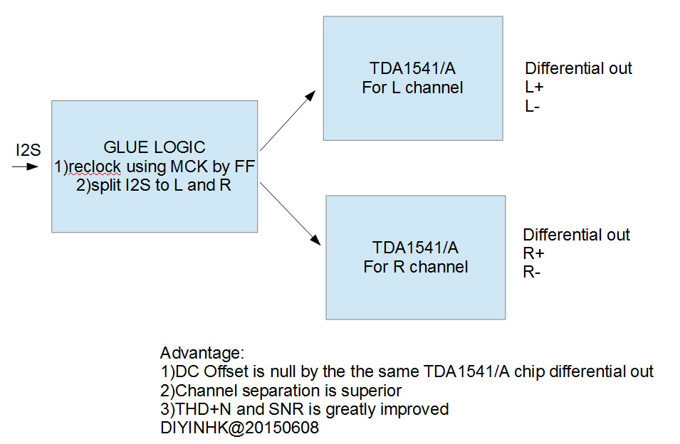
The goal of this project is TDA1541A differential out NOS DAC with standard i2s input.
The XMOS official audio reference design also has a FF to reclock the SPDIF output. There are something that must be done by hardware circuit rather than firmware programming. The reason is described in the USB Audio Design Guide 3.7.1 There are 2.5-5ns jitter in the output of xmos, reclock using a FF can eliminated the jitter
This project uses the same jitter removal method, as the output quality of R2R type DAC greatly depends on the jitter of BCK and LRCK, 2.5-5ns is unacceptable for audiophiles, the input will use a FF to reclock the BCK and LRCK to remove the jitter.
Even a real time XMOS processor has 2.5-5ns jitter on it's output, all CPLD base type usb i2s module should also have the same problem, i.e. all 3 wire i2s input R2R DAC should be reclocked by the MCK/OSC or bad sound.
Delta-sigma DAC is another world, they have 4 wire i2s input and it's already includes MCK/OSC input.
My preferred approach for a new development is to request a XMOS code owner / developer to make a board that directly provides the requested simultaneous output.
We are commonly seeing a USB converter as a black box with definite code in EEPROM; however it is not.
It is « easy » for instance if you buy a demonstrator board from the factory and allowed to write your own code.
Not many can do that.
But One stands out: Lucien of Romega Fame.
The board the XMOS is implemented on of course then needs different peripherals (such as an added output) from a standard USB converter, but it is not too different at all in my opinion.
My 2 ¢
albert
Last edited:
I have been using a dual 1541 nos dac reconfigured by inverting the data to one dac as Marantz have done and using a pair of Sowter 9545 transformers bifilar would, differentially connected, with 100R I/V resistors and no other filtering. It sounds excellent but I would have been interested in comparing with the OP's way. I prefer the sound to an Audio Note AD1865 dac using the same transformer in single ended mode.There is nothing wrong with the Marantz approach, although I don't see the point in making a differential signal by two DAC chips, and then combine them to unbalanced.
I am planning to use a centre tapped transformer fed by the differential signal.
I suspect the extra glue logic and potential for additional jitter will cancel out the sonic benefits.
I have been using a dual 1541 nos dac reconfigured by inverting the data to one dac as Marantz have done and using a pair of Sowter 9545 transformers bifilar would, differentially connected, with 100R I/V resistors and no other filtering. It sounds excellent but I would have been interested in comparing with the OP's way. I prefer the sound to an Audio Note AD1865 dac using the same transformer in single ended mode.
I suspect the extra glue logic and potential for additional jitter will cancel out the sonic benefits.
Actually, the real way to fight jitter is glue logic! Many people may already confused by some marketing topic. The output of all FPGA, CPLD(such as altera max ii)contains huge amount of jitter and if it is used for serious audio, you should found glue logic circuit on it's output to eliminate the jitter.
- Status
- This old topic is closed. If you want to reopen this topic, contact a moderator using the "Report Post" button.
- Home
- Source & Line
- Digital Source
- The Best TDA1541A differential out NOS DAC