Hi rfbrw
If I get right, You said that :
DAC receveing first left word data,
keaping the word in memory,
then wait for the next word right word,
and then go to conversion of booth words in same time..?
And it still I dont know which of the digital datas in the data bus corresponding to
L/L- or R/R- analog outputs..?
Please explain to me...Thanks in advance.
Rah,
I haven't tried the modified circuit, in part because of a somewhat limited enthusiasm for this mode of operation but mainly because I see nothing in the timing diagrams that would put the two datastreams in the same timeframe as shown in the your attached snippet of the TDA1541A datasheet. What I do see is something not dissimilar to what Burr-Brown call stopped clock mode or burst clock i.e. you have just enough cycles to load the relevant serial register. But to support burst clock operation separate serial clock inputs are essential and the TDA1541A lacks them so one must conclude that the left and right datastreams must be in the same timeframe for the simultaneous mode of operation to work.
“When input OB/TWC input is connected to VDD1 the two channels of data (L/R) are input simultaneously via DATA L and DATA R, accompanied with BCK and a latch-enable input (LE). With this mode selected the data must be in offset binary. "
ray
Zoran said:Hi rfbrw
If I get right, You said that :
DAC receveing first left word data,
keaping the word in memory,
then wait for the next word right word,
and then go to conversion of booth words in same time..?
Correct
And it still I dont know which of the digital datas in the data bus corresponding to
L/L- or R/R- analog outputs..?
Please explain to me...Thanks in advance.
You can have one dac with L and R data or one dac with L and L- or R and R- data but not one dac with L/L- and R/R- data. For that you need two dacs. You send one dac L and L- and the other R and R-. A normal I2S signal from the CS8412 is L/R L/R L/R.... so you need to make two I2S signals of L/L- L/L- L/L- and R/R- R/R- R/R-. So on on dac the analogue output will be AOL = L and AOR = L- on the other it will be AOL = R and AOL = R-.
ray.
Sorry that I am send post messages frequently...
But for Me in completly new light about the converting procedure that informations i get is from vital importance
...Now I see : technicaly no matters which format we use for feeding the TDA1541A
becouse in all 3 cases of input formats DAC did not starts conversion until get L word and after that R word...Now it seems : becouse we already
(in numerous cases)
have the classic I2S bus, it is the most conviniant way to split the bus and after that to split phases if we want to
have split Power supplys on each chanels from the beguening?
Ray,
Yup, that's right... it is similar to the stopped clock mode.
Ah, but we do have separate serial clock inputs. One on each TDA1541A. If you look at the first circuit I posted, the XOR gates invert the data to give you the opposite phase. So from LDATA, you get L+ and L- both of which are in the same timeframe. And the same goes for R+ and R-.
Visualize the connections:
TDA1541A Chip A outputs L+ on it's left output pin and L- on it's right output pin. It gets L+ digital on it's DATAL pin, and L- digital on it's DATAR pin. L+ and L- are both in the same timeframe, as they are derived from the Left data burst, and simultaneously enter TDA1541A Chip A with one clock LCK.
TDA1541A Chip B outputs R+ on it's left output pin and R- on it's right output pin. It gets R+ digital on it's DATAL pin, and R- digital on it's DATAR pin. R+ and R- are both in the same timeframe, as they are derived from the Right data burst, and simultaneously enter TDA1541A Chip B with one clock RCK.
What I do see is something not dissimilar to what Burr-Brown call stopped clock mode or burst clock i.e. you have just enough cycles to load the relevant serial register.
Yup, that's right... it is similar to the stopped clock mode.
But to support burst clock operation separate serial clock inputs are essential and the TDA1541A lacks them...
Ah, but we do have separate serial clock inputs. One on each TDA1541A. If you look at the first circuit I posted, the XOR gates invert the data to give you the opposite phase. So from LDATA, you get L+ and L- both of which are in the same timeframe. And the same goes for R+ and R-.
Visualize the connections:
TDA1541A Chip A outputs L+ on it's left output pin and L- on it's right output pin. It gets L+ digital on it's DATAL pin, and L- digital on it's DATAR pin. L+ and L- are both in the same timeframe, as they are derived from the Left data burst, and simultaneously enter TDA1541A Chip A with one clock LCK.
TDA1541A Chip B outputs R+ on it's left output pin and R- on it's right output pin. It gets R+ digital on it's DATAL pin, and R- digital on it's DATAR pin. R+ and R- are both in the same timeframe, as they are derived from the Right data burst, and simultaneously enter TDA1541A Chip B with one clock RCK.
Rah
I done some "research" according to the
Philips datas of TDA1541A...
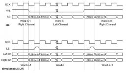
Putting together in a simbolic way the input fomats fraphs of I2S & simultaneously LR mode...
First I saw is that SCLK of the sim. mode is inverted (look at the MSB of words...)
and LE is still prior to the MSB...seems changing state only for the half of period of the SCLK...
Second and from the more importance is that looking at sim. mode bus implicates that dac go to conversion LR chanels literary simultaneously...
Third : I think that we have a good chance to use pair of DACs left bus goes to L & R of first DAC (out is Left un-balanced but parallel), and right goes to L & R of second DAC (out is Right un-balanced but parallel),
*
I did not get the answer about the
balanced output which bit or bit complement or ...I dont know is corresponds to +phase or -phase at the audio output of the dac...
*
please take a look at the diagram...
Thanks
I done some "research" according to the
Philips datas of TDA1541A...
Putting together in a simbolic way the input fomats fraphs of I2S & simultaneously LR mode...
First I saw is that SCLK of the sim. mode is inverted (look at the MSB of words...)
and LE is still prior to the MSB...seems changing state only for the half of period of the SCLK...
Second and from the more importance is that looking at sim. mode bus implicates that dac go to conversion LR chanels literary simultaneously...
Third : I think that we have a good chance to use pair of DACs left bus goes to L & R of first DAC (out is Left un-balanced but parallel), and right goes to L & R of second DAC (out is Right un-balanced but parallel),
*
I did not get the answer about the
balanced output which bit or bit complement or ...I dont know is corresponds to +phase or -phase at the audio output of the dac...
*
please take a look at the diagram...
Thanks
Attachments
Of course first we have to design a propper interface...to convert the I2S to sim. LR.
Note: I don't know any other DAC using the same input format even as a mono chip...maybe it is much effort to design a interface just for the one chip no matters how the TDA1541A is good..?
Note: I don't know any other DAC using the same input format even as a mono chip...maybe it is much effort to design a interface just for the one chip no matters how the TDA1541A is good..?
Zoran said:Of course first we have to design a propper interface...to convert the I2S to sim. LR.
Note: I don't know any other DAC using the same input format even as a mono chip...maybe it is much effort to design a interface just for the one chip no matters how the TDA1541A is good..?
TDA1540 (?) mono DAC, but then only 14 bit
GuidoB
Yes Guido
but I saw the data sheets of the TDA1540
and there is 3 Vref pins and few pins for the osc. I think.
It will be real play to set all those values...
But I heard the TDA 1540 once in some old philips CD player (I think CD101...)
a little silver coulered front...
and it sounds beautifuly...
maybe a little bit soft almost like vinil...
And I think that is hard to find those chips.
You were only talking about the 'input format'. Not about all the other pins etc to get it working..
Anyway, i've got a working B&O CD-X with those DAC's (and CDM1 transport). It is a philips CD104 in a really nice package.
Not going to mod it (difficult, no space etc) but keep it as as it is.
Greetings,
Anyway, i've got a working B&O CD-X with those DAC's (and CDM1 transport). It is a philips CD104 in a really nice package.
Not going to mod it (difficult, no space etc) but keep it as as it is.
Greetings,
Zdravo Zorane,
I am trying to figure what is the goal here. To make the TDA1541A working in the simultaneous mode, for the sake of the knowledge & experience? To make two DAC chips unit, with each chip dedicated for one channel only, thus getting supposed benefits of going separate supply for each channel’s DAC? Or to make the DAC working in balanced mode? Or last two both?
If the balanced mode is still not what you intend to do (as you said in the post #12) and you want just a separate DAC chip for each channel thus you can use a separate supplies for them, why don’t you feed two DAC chips with the same I2S and tap the output for one channel from the one DAC chip and the other output from the other’s channel output of the other DAC chip? If you want to make each chip quiet for the anyway unused channel, I guess one HC157 and one inverter can accomplish this.
To go balanced (you still seem to be interested for this in the post #28) and maybe to get some other ideas, it is not bad to check this thread (if you did not do that already):
http://www.diyaudio.com/forums/showthread.php?s=&threadid=20867
Yes, according to the Philips’s drawing, in the simultaneous mode the data is latched on the trailing edge of the bit clock.
Seems like that but it might be also helpful if someone can point to the place where the simultaneous mode is explained better than in the Philips’s datasheet.
Yes, but from the practical point of view, DAC anyway do the conversion simultaneously, i.e. at one hand there is always some kind of buffering and at the other hand the output signal always appears at the outputs at the same time. The format of the incoming signal doesn’t change this.
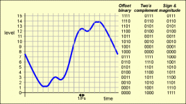
If you ask about the structure of the data, have a look here:
http://web.onetel.net.uk/~peterphmusic/pharri5833/digaudio.htm
(check the 4th figure)
If you ask about the way to get the inverted signal at the output, inverting of the data line of the two’s complement is probably the easiest way.
Pedja
I am trying to figure what is the goal here. To make the TDA1541A working in the simultaneous mode, for the sake of the knowledge & experience? To make two DAC chips unit, with each chip dedicated for one channel only, thus getting supposed benefits of going separate supply for each channel’s DAC? Or to make the DAC working in balanced mode? Or last two both?
If the balanced mode is still not what you intend to do (as you said in the post #12) and you want just a separate DAC chip for each channel thus you can use a separate supplies for them, why don’t you feed two DAC chips with the same I2S and tap the output for one channel from the one DAC chip and the other output from the other’s channel output of the other DAC chip? If you want to make each chip quiet for the anyway unused channel, I guess one HC157 and one inverter can accomplish this.
To go balanced (you still seem to be interested for this in the post #28) and maybe to get some other ideas, it is not bad to check this thread (if you did not do that already):
http://www.diyaudio.com/forums/showthread.php?s=&threadid=20867
Zoran said:First I saw is that SCLK of the sim. mode is inverted (look at the MSB of words...)
Yes, according to the Philips’s drawing, in the simultaneous mode the data is latched on the trailing edge of the bit clock.
and LE is still prior to the MSB...seems changing state only for the half of period of the SCLK...
Seems like that but it might be also helpful if someone can point to the place where the simultaneous mode is explained better than in the Philips’s datasheet.
Second and from the more importance is that looking at sim. mode bus implicates that dac go to conversion LR chanels literary simultaneously...
Yes, but from the practical point of view, DAC anyway do the conversion simultaneously, i.e. at one hand there is always some kind of buffering and at the other hand the output signal always appears at the outputs at the same time. The format of the incoming signal doesn’t change this.
I did not get the answer about the
balanced output which bit or bit complement or ...I dont know is corresponds to +phase or -phase at the audio output of the dac...
If you ask about the structure of the data, have a look here:
http://web.onetel.net.uk/~peterphmusic/pharri5833/digaudio.htm
(check the 4th figure)
If you ask about the way to get the inverted signal at the output, inverting of the data line of the two’s complement is probably the easiest way.
Pedja
rah said:Ray,
One on each TDA1541A.
Rah,
Arrgh.Overlooked that Anyway built it and with the exception of some reversed signals it worked in the simulator. Sent bitstream to FPGA and configured it. Connected to CS8412. Ah too many SCLK cycles. Currently working on that. You design assumes SCLK of 32Fs. CS8412 has SCLK of 64Fs.
Hi Pedja
I wisit the address You post...
Yes You are right
the aim is to put the (2n) TDA1541A
(or maybe the TDA1543 ) in separate chanels mode (vith a possibility to choose beetwen the unbalanced and balanced output)and separate chanels power suplys...From the I2S data bus
but if it is somehow posibile to acomplish this without the programmed procesor supervisionn...
Attachments
About the spliting phases or balancing...
I2S bus is a time multiplexed as well as
twos complement data format (see the picture )
TDA1541A in simultaneous L/R input mode expects data in off-set binary form...
Another thing : simple inversion of data bus throught inveter or throught reclocking flip-flops elements will give the uncorrect results even in I2S mode...
first becouse of fact that WS goes prior one clock cycle to the MSB and we always loosing the LSB of each word making the LSB of one chanel go to another...
*
As I see from the picture only the MSB of data word is important like information about phase...other bits are values of signal or magnitudes..?
*
please comment...
Arrgh.Overlooked that Anyway built it and with the exception of some reversed signals it worked in the simulator. Sent bitstream to FPGA and configured it. Connected to CS8412. Ah too many SCLK cycles. Currently working on that. You design assumes SCLK of 32Fs. CS8412 has SCLK of 64Fs.
Ray,
Yes, that was silly of me.. since my CDROM transport outputs 48Fs and the the CS8412 outputs 64Fs.
A counter to count the bits has to be added. It would have to stop after 16 bits so that the trailing bits don't flush out the first 16. I'll get working on it soon, if ya get it to work before then, let us know
")
Another thing, sorry for the slow replies (I've been busy). Unfortunately they'll be even slower now cause my DSL has gone down, and it's not comming back up for at least a week
(I'm using my work's network, by dial-up atm)
rah said:
Ray,
Yes, that was silly of me.. since my CDROM transport outputs 48Fs and the the CS8412 outputs 64Fs.
A counter to count the bits has to be added. It would have to stop after 16 bits so that the trailing bits don't flush out the first 16. I'll get working on it soon, if ya get it to work before then, let us know
Another thing, sorry for the slow replies (I've been busy). Unfortunately they'll be even slower now cause my DSL has gone down, and it's not comming back up for at least a week
(I'm using my work's network, by dial-up atm)
Rah,
Added the counters and it simulates correctly. Will try it with a real TDA 1541 and a FPGA later today but thats as far as I'll go. Started to convert from individual logic gates to 74 series packages but as the logic to create the 1:3 mark/space ratio signal alone looked like it would take 5 packages, I knocked it on the head. As I have a cmos/ttl board somewhere that alledgedly creates balanced I2S, I'll dig that out and see if it actually does anything.
ray.
- Status
- This old topic is closed. If you want to reopen this topic, contact a moderator using the "Report Post" button.
- Home
- Source & Line
- Digital Source
- TDA_1541A input formats