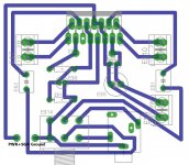
I would move the right channel input cap to the other side of the PCB and connect the right input to the chip from that side.
I would also remove the s-gnd/p-gnd connection track completely, and connect the signal ground from the input connectors GND to the power connectors GND, using the low value resistor as the jumper...
Also when entering the signal in to the chip from the left side, use the input capacitors as jumpers to get pass the s-gnd track. Much shorter signal tracks that way - which I find importan.
Are you using the signal ground for the mute control circuitry? Use power ground for that.
Last edited:
I would move the right channel input cap to the other side of the PCB and connect the right input to the chip from that side.
I would also remove the s-gnd/p-gnd connection track completely, and connect the signal ground from the input connectors GND to the power connectors GND, using the low value resistor as the jumper...
Also when entering the signal in to the chip from the left side, use the input capacitors as jumpers to get pass the s-gnd track. Much shorter signal tracks that way - which I find importan.
Are you using the signal ground for the mute control circuitry? Use power ground for that.
Thank you for your valuable input, will do and post the new layout here soon.
")
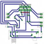
Not bad...
Turn the cap E1 90degrees left and you will get that part of the pcb even nicer.
You could also move the ground track from between the input channels via the bottom side of the pcb to the power connector.
And you could try to move the components abit here and there and see how tiny you can get the PCB now.
Even though AndrewT is against it, if this were my PCB, I could put ground fills around the outputs and the power input tracks.
Also, make the output tracks and the power tracks as wide as possible.
Not bad...
Turn the cap E1 90degrees left and you will get that part of the pcb even nicer.
You could also move the ground track from between the input channels via the bottom side of the pcb to the power connector.
And you could try to move the components abit here and there and see how tiny you can get the PCB now.
Even though AndrewT is against it, if this were my PCB, I could put ground fills around the outputs and the power input tracks.
Also, make the output tracks and the power tracks as wide as possible.
And leave supply rails thin as possible?
Not bad...
Turn the cap E1 90degrees left and you will get that part of the pcb even nicer.
You could also move the ground track from between the input channels via the bottom side of the pcb to the power connector.
And you could try to move the components abit here and there and see how tiny you can get the PCB now.
Even though AndrewT is against it, if this were my PCB, I could put ground fills around the outputs and the power input tracks.
Also, make the output tracks and the power tracks as wide as possible.
Thanks a lot for your input, i intend to use a ground fill just didn't add it yet. I will rotate the input capacitor as you mentioned but the power ground trace unfortunately isn't going anywhere
as the ground path near the PCB bottom is the signal ground, again thank you for your advice.Cool as the other side of the pillow.And leave supply rails thin as possible?
- Status
- This old topic is closed. If you want to reopen this topic, contact a moderator using the "Report Post" button.
- Home
- Amplifiers
- Chip Amps
- TDA7297 Board Layout Suggestions