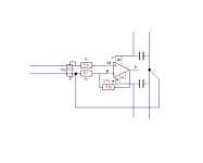
Nothing more confusing than a feedback loop. When I started playing with these chips it seemed logical to connect Ri to power/output return as part of the feedback loop and treat Ri's function as part of the input loop as secondary (high current over low current). Tomchr measurements convinced me that the inputs and their resistors should be configured as twins, that a small amount of resistance/inductance between input return and power/output return is not a problem, maybe even adds to HF stability and reducing ground noise/loops.
re post97 neurochrome link
i.e. both connected to the Signal Source.
Most of the earlier diagrams show the very confusing use of a three bar ground symbol.
After this diagram he says
He has kept the Signal route as TWO wires and the Load route as TWO wires and added that important voltage reference connection.
What he did NOT do is take the Signal Return to the Output instead of to the Source.
The diagram that follows this shows the TWO inputs labeled as GND_SIG and GND_SIG.From a feedback theory point-of-view, it seems apparent that if the voltage across the load is what we intend to control, the feedback voltage should be measured as close to the load as possible. This means that GND_SIG should connect to GND_LOAD.
i.e. both connected to the Signal Source.
Most of the earlier diagrams show the very confusing use of a three bar ground symbol.
After this diagram he says
he has made a Signal Return/Ground voltage reference connection to the Load Return/Ground.Bingo! Now 1 A of returning load current will result in 100 nV (-140 dBV) of error voltage developed across the load for DC signals. Even at 10 kHz, the error voltage is only about 56 µV (-85 dBV) – a 40+ dB improvement over the star grounding scheme at 10 kHz and 95 dB improvement near DC. The only difference between the star ground and the improved grounding scheme is that the GND_SIG trace was routed to the output connector rather than to the star ground.
He has kept the Signal route as TWO wires and the Load route as TWO wires and added that important voltage reference connection.
What he did NOT do is take the Signal Return to the Output instead of to the Source.
Last edited:
absolutely.Tomchr measurements convinced me that the inputs and their resistors should be configured as twins,
EVERY circuit must be treated as TWINS. Use twisted pairs everywhere. Since a PCB can't implement twisted pairs the best we can use is close coupled pairs.
One trace over another trace with a 6mil to 10mil insulation layer is as good as we get at the moment.
59mil (the thickness of a 1.5mm thick double sided PCB) or 63mil (1.6mm) is not close coupled. But it's a lot better than separating the twin into two different Flow and Return routes.
That does not explain the apparent indifference to the larger loop of the relatively higher current of the feedback loop, also a flow and return circuit.
V+/-, chip, output, Rfb, Ri, Ci, PGND, V+/-.
I tried to understand the sims used by tom for measuring ground noise so I could use the method for my own sims. I came to the conclusion that because the power supply used was too perfect the method was possibly incomplete.
V+/-, chip, output, Rfb, Ri, Ci, PGND, V+/-.
I tried to understand the sims used by tom for measuring ground noise so I could use the method for my own sims. I came to the conclusion that because the power supply used was too perfect the method was possibly incomplete.
in trying to import tom's results to this (7293 board) context we face the additional uncontrolled variable that the grounding scheme here does not appear to me to closely resemble anything tom tested. for example, (ignoring the slave for a moment) consider the trace beginning at master pin 4, progressing to pin 1 then to the standby cap return then to the NFB shunt cap return then to the input ground then to the rails ground then to the output ground.
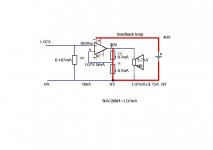
Does the feed back loop have a much higher current?
The current is limited by the impedance of the two feedback resistors and the output voltage. eg a 27k+1k NFB network driven by a 3Vpk signal draws 0.107mApk
If the feedback resistors are kept very close to the respective Flow Currents then each loop will be small and thus emitted and received interference will be small.
true enough. the signals sharing the "buss" are all relatively low current so it's not anything like having a speaker return in the middle of it -- speaker return is on the other side of the PSU return and the bypass capacitors so it's aside from the path of these lower current signals. if the entire FB network (2 Rs and a C) is located close to pins 1,2 and 4, then the rest of it may not matter much.
Last edited:
Does the feed back loop have a much higher current?
The current is limited by the impedance of the two feedback resistors and the output voltage. eg a 27k+1k NFB network driven by a 3Vpk signal draws 0.107mApk
If the feedback resistors are kept very close to the respective Flow Currents then each loop will be small and thus emitted and received interference will be small.
Feedback current is output voltage / R
30 Vpk / 28 k = 1.0714 mApk
Input Bias current = 1uA (max)
The max source current depending on the resistors used at the input will be about 0.05 to 0.1 mApk
Last edited:
When it's unity gain the voltages and the resistances are the same.
The currents end up the same and the Flow field cancels the Return field.
But when I draw a 28times gain amp, the voltages don't match, as expected.
That results in currents that don't match.
I can't see it at the moment. I'm missing something.
The currents end up the same and the Flow field cancels the Return field.
But when I draw a 28times gain amp, the voltages don't match, as expected.
That results in currents that don't match.
I can't see it at the moment. I'm missing something.
exactly. the psu sources a total of 3.75107A to the chip V+ pins. the chip pin 3 sources that same amount of which 3.75A goes to the load and the rest gets sunk into the FB divider to develop the voltage fed to pin 9. pin 9 and 10 are at the same potential. all's right with the world. am i missing something here?
Different current needed? If power voltage is 35+35vdc, the gain divider can be either 47k vs 1k2 or 27k vs 730, and it can be set lower if using lower voltage.
With 47k vs 1k2, a somewhat more convenient size fb-shunt coupling cap can be used series to the 1k2, because values larger than 680u wouldn't be very useful. Even 470u may work passably (if when the +in cap is small enough) and lower voltage models don't take up much space on the board.
Or, starting with measuring equipment (even as simple as RMAA) and 33k vs 1k0, it is possible to shelve the gain (rc added to the 1k0) conservatively (and carefully measured) to compensate for the slight treble droop, so then you have somewhat, almost, normal gain.
Or, what really needs to be explored is using the TDA7293 at inverting mode to see if that allows lower gain as expected.
I did try almost every resistor value in non-inverting mode (yes, soldered every one of them), but have not yet tried inverting mode.
I can't argue with that.
The two input wires carrying 107uA must be a close coupled pair.
The next two input wires carrying 0mA (but actually 0.xuA) also need to be a close coupled pair.
The two speaker wires carrying 3.75A need to be a close coupled pair.
The two wires carrying the 3.75107A (the Supply wires) must be a close coupled pair. BUT in addition the unbalanced current, between the +ve and -ve supplies has to flow along the Power Ground wire and that has to be combined with the supply wires to make a power TRIPLET.
So back to where I was at before I became confused:
Every Flow and Return PAIR must be close coupled to minimise the interference.
Last edited:
Schematic @#114 was for AndrewT.
Here is a better schematic for PCB layout. It is based on Tomchr "IN+FB long GND" version.

As you can see the flow and return theory does not explain the improvement, I(Ri) is much higher than I(Rb). Flow and return ends beyond Rin.
A possibly better explanation: Think of the two inputs as voltage measuring devices and therefore the inputs need to have the same ground reference, but I'm only guessing.
Here is a better schematic for PCB layout. It is based on Tomchr "IN+FB long GND" version.

As you can see the flow and return theory does not explain the improvement, I(Ri) is much higher than I(Rb). Flow and return ends beyond Rin.
A possibly better explanation: Think of the two inputs as voltage measuring devices and therefore the inputs need to have the same ground reference, but I'm only guessing.
How are you attaching the sch/diagram?
It links to a new tab which means I can't look at the comment alongside the sch.
Most attachments open on the same page and can be moved so that I and others can see the attachment while typing a reply or reading comments, even a comment/explanation in a different post.
It links to a new tab which means I can't look at the comment alongside the sch.
Most attachments open on the same page and can be moved so that I and others can see the attachment while typing a reply or reading comments, even a comment/explanation in a different post.
Last edited:
- Home
- Amplifiers
- Chip Amps
- TDA7293 Parallel kit from ebay (modular/slave style, no lossy emitter resistors)
