Re: !
Hi Viktor,
It's good to hear you got help from Boraomega!
Would you like to post the modified schematic by Boraomega, it would be very kind of you and probably appreciated for several of those who tried to give you hint's and others too to see your new schematic, thanks!")
Cheers Michael
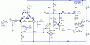
viktor1986 said:Boraomage sent me modifyed schematic.Thank's everybody
Sorry for my bad english!
Hi Viktor,
It's good to hear you got help from Boraomega!
Would you like to post the modified schematic by Boraomega, it would be very kind of you and probably appreciated for several of those who tried to give you hint's and others too to see your new schematic, thanks!
Cheers Michael
HarryDymond said:Looks like it's in the wrong place, one end should be connected to the collector of Q10, the other to the junction of R13, C2, R17, D3 and R2 to R5.
I forgot to say that if a resistor were placed in this position, you'd expect it to have a value around 20 ohms. Its purpose would be to reduce the variations in voltage across the Vbe multiplier caused by varying current.
AndrewT said:Harry
can you recall or prepared to take the time to tell us which diags were wrong?
I should clarify and say that it was quite a few years ago that I read the book and it is just my recollection that there were errors. I could be wrong. I guess I'm just surprised by your reaction to the H&H book, I've never met anyone who doesn't think it's great!
Hi Viktor,
thanks for posting the schematic and thanks to Boraomega who made the changes and gave the permission.
I think this is now a good basic amplifier that anyone can build.
Viktor, you had 4 pair of output transistors in your schematic, but in Boraomegas improved schematic there's only one pair, but the voltage still remains at +-60V, how many output transistor pairs does Boraomega suggest this amplifier can work with?
I do notice VAS has a high bias current though...
Good luck with your amplifier!
Cheers Michael
PS: It would be nice to see Boraomega here on this forum!
Ultima Thule said:I think this is now a good basic amplifier that anyone can build.
Viktor, you had 4 pair of output transistors in your schematic, but in Boraomegas improved schematic there's only one pair, but the voltage still remains at +-60V, how many output transistor pairs does Boraomega suggest this amplifier can work with?
I do notice VAS has a high bias current though...
Good luck with your amplifier!
PS: It would be nice to see Boraomega here on this forum!
ditto
What is the purpose of C8? Presumably it shorts very high frequencies to ground better than the eletrolytic, but is that necessary?
!
I really don't know how many output transistors suggest Boraomega!
Thank's!
Ultima Thule said:Hi Viktor,
thanks for posting the schematic and thanks to Boraomega who made the changes and gave the permission.
I think this is now a good basic amplifier that anyone can build.
Viktor, you had 4 pair of output transistors in your schematic, but in Boraomegas improved schematic there's only one pair, but the voltage still remains at +-60V, how many output transistor pairs does Boraomega suggest this amplifier can work with?
I do notice VAS has a high bias current though...
Good luck with your amplifier!
Cheers Michael
PS: It would be nice to see Boraomega here on this forum!
I really don't know how many output transistors suggest Boraomega!
Thank's!
Hi Victor1986,
Your amp will need 2pairs of MOSFETs for this supply.
Also bias T comp will be 2 x too severe. You could make half the 2Vgs with a resistor or put one on the emitter leg of the bias BJT.
You don't really need 2N5401 for input with 60V and would do better with a high Hfe type to reduce bias currents. Your Vas comp is a bit primitive. why not 2 pole it to improve PSRR and HF THD.
Clipping will not be symmetrical due to 6V loss on negative swing but only 1V Vsat on positive. Still plenty swing though.
Cheers,
Greg
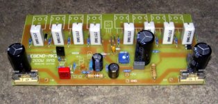
Hello Viktor,
that looks very nice! ..but it looks like you have not every component on PCB according to the silkscreen.
Is it possible to see a good picture from soldering side so we can see the nice layout of your PCB?
Now we wonder how does it sound, get it finnished/connected and tell us!
BTW, where did you get your PCB's manufactured and how much did you pay for them?
Cheers Michael
Re: !
its more cheap here.same pcb can be done for $3 each
must say,very nice.
how does it sound!
viktor1986 said:I paid 10euro for two PCB!!!Really cheap.In my country(Serbia) 1dm^2 is 2.5e.
its more cheap here.same pcb can be done for $3 each
must say,very nice.
how does it sound!
Re: !
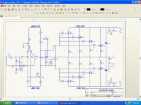
Probably it can 'function'.
If it would give an excellent performance, this is more questionable.
What can be critical is the current through Q3.
15 mA is good for driving 1 big MOSFET.
Because BIG MOSFET has input capacitance, they 'suck' current.
15 mA / 4 MOSFET = 3.75 mA per device
3.75mA is a lot less than 15 mA.
I would like to have 10 mA per MOSFET.
This would need to increase Q3 current to 40 mA.
How much you should use here for best result, I think other know better.
You might need to use 2 transistors darlington for Q3.
Otherwise the input stage with only 1.5 mA per transistor
will maybe have difficult drive Q3. If using 40 mA in Q3.
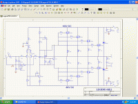
viktor1986 said:Hi…
The original schematic is Legend1.
If I want more power could I use Legend2(picture two)?
Please…
Probably it can 'function'.
If it would give an excellent performance, this is more questionable.
What can be critical is the current through Q3.
15 mA is good for driving 1 big MOSFET.
Because BIG MOSFET has input capacitance, they 'suck' current.
15 mA / 4 MOSFET = 3.75 mA per device
3.75mA is a lot less than 15 mA.
I would like to have 10 mA per MOSFET.
This would need to increase Q3 current to 40 mA.
How much you should use here for best result, I think other know better.
You might need to use 2 transistors darlington for Q3.
Otherwise the input stage with only 1.5 mA per transistor
will maybe have difficult drive Q3. If using 40 mA in Q3.
- Status
- This old topic is closed. If you want to reopen this topic, contact a moderator using the "Report Post" button.
- Home
- Amplifiers
- Solid State
- Take a look on amplifier schematic please