theChris said:you may concider using a lm4780 or 4732.
I have an amp with LM4780.
Regulated - buffered - NIGC...
Joe Rasmussen said:Do I hear a business proposal?

Joe, I just said it would be interesting to measure the chips and match them before using them.
Maby the ones you have with lower DC have something in common?
Pedja said:
Hi Sheldon,
It is simlar to the NIGC. The impedance here is mainly determined by the first series resistor. This 22k instead of 10k will shift the slope a bit down, and to keep the previous slope you may use somewhat lower value for the first resistor. Something like 900R instead of 1k will be fine.
Pedja
Ah yes, I should have seen the analogy. Thanks. I'll get better at this eventually.
Sheldon
Pedja said:
Yes, with typical bias current and if the first resistor is higher than 10k, offset developed by the bias current will start to dominate over rather than it will null the contribution of the input offset voltage. So, I’d stop here at 10k.
Yes, it will cope with a greater spread, even if it won't get the lowest offset with the typical chips. In this case I am of the same view that it is the bias offset current that is the culprit rather the offset voltage. 10K it is then.
Pedja said:
These values may be good either for tube or solid state buffers or no buffers at all.
As a final result, I doubt the offset at the output will come higher than 50mV. Though it will vary below this point more than we accustomed to...
Yes. If I may quote Terry quoting Pass:
Nelson Pass says of his amps (which are DC coupled, sans servos) that he is happy to get 50mV offset at OP and they are specced at max 100mV.
Proceeding on that basis, shall there be a general consensus to the values shown below? One will be the proposed CF circuit with LPF I will amend to my DIY website and the other just showing a generic buffer with straight 22K Input Z.
An externally hosted image should be here but it was not working when we last tested it.
Now the generic buffer view, insert the buffer of choice, no LPF but that is easily optional by splitting the 22K Input Z with 3K9, 1n5 tweaked, 18K as above.
An externally hosted image should be here but it was not working when we last tested it.
Joe R.
Franz G said:Monday morning, back on the net...
Great what you worked out! Thanks!
Joe: why do you use a coupling cap in the chip buffered version?
Franz
It's not really a 'chip' - as it is generic it could a Pedja's J-fet buffer, which has some DC on it - and he has nominated 4u7 value. Even if it is a chip, how many mV Offset would have? If only 2mV then multiply that by 45 and you've added 90mV Offset. But if you have an IC with zero Offset without drift, then by all means ditch it. But I suspect in 95% plus cases you will need it.
Joe R.
If only 2mV then multiply that by 45 and you've added 90mV Offset.
And if you have >600mV (like I have with my discrete buffer) then you need a calculator as well as the cap!
Nuuk said:
And if you have >600mV (like I have with my discrete buffer) then you need a calculator as well as the cap!
Seriously though, have you turned on your VIGC without the necessary delay, and straight away heard a loud buzzzzz?
What is actually happening is the amp pushed to it rail (negative if I remember right) and the buzz you hear is actually the ripple on the neg rail until the voltage settles down.
What would happen if you had about -0.8V approx on the buffer (the cathode in fact) go straight through? Inverted and multiplied by fourty odd and now the positive rail straight through to the speaker since 0.8V x 45 = 36V - in fact the supply will sag to near 30V. That and a loud power supply ripple (buzz) on the output. Be quick or...
... throw your speaker a goodbye kiss.

I know this happens because I had a cap fail - short. Quick action and voice coil still in tact.
Joe R.
Seriously though, have you turned on your VIGC without the necessary delay, and straight away heard a loud buzzzzz?
Sorry Joe, I was referring to my discrete transistor buffer shown here .
If I am not using a speaker protection module with a power on delay (as is the case with the VBIGC), I always turn on my buffers before powering up the power amp sections.
While on this subject, I have a cunning plan to prevent both sections powering up together in the event of a short mains supply break. I'll put it up on a new thread for comments (or ridicule
) as I am not sure if it will work. 
Nuuk said:
Yep, that circuit would have near negative 0.6V before cap.
While on this subject, I have a cunning plan to prevent both sections powering up together in the event of a short mains supply break. I'll put it up on a new thread for comments (or ridicule
Mate, I think I've put my foot in it a few times on these forums, but alas I cannot go over my past postings and edit them. But life on a high wire is more fun and in this case the potential harm rather less.
:I too am working on a simple idea that will be preventative in case somebody forgets the delay or they get an unexpected interuption to the mains supply - but I want to be sure it has no bad sonic effects first. The idea will slow down the voltage spike and its level, at least preventing it hitting the rail voltage which is when the buzz comes in. So you will see some cone wobble but little or no sound. It worked pre-T-network, now need to try it again. Should work the same, but also needs a good listen. Only two additional components per channel - we're talking VIGC application here.
Joe R.
Don't see why it couldn't be done with NIGC, but it's not so important, since you can use a 20k feedback resistor and 20k from input to ground - already reasonably low values. Don't know why any preamp or buffer would cause a problem. If anything, should make life easier. Experts chime in here if I'm mistaken.
I wonder if the lower values commonly used on the NIGC are partly responsible for some users preference for this topology prior to the T?
Sheldon
I wonder if the lower values commonly used on the NIGC are partly responsible for some users preference for this topology prior to the T?
Sheldon
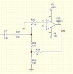
Have you tried a compromise like the one on the sch. I'm attaching here? That should be better if the high input Z is not as important as in the old post bellow. The DC gain is only 10 (or 5) instead of 100, thus matching R16 and R22 is 10 times less critical. The rest of the gain comes from R16/R27 (on the attached sch). So you get reasonable NFB resistor of 47k and a good DC offset.
Ignore the OPAMP type, please. It was for simulation purposes only.
The older post:
http://www.diyaudio.com/forums/showthread.php?s=&threadid=33266
/Greg
Ignore the OPAMP type, please. It was for simulation purposes only.
The older post:
http://www.diyaudio.com/forums/showthread.php?s=&threadid=33266
/Greg
Attachments
GregGC said:Have you tried a compromise like the one on the sch. I'm attaching here? That should be better if the high input Z is not as important as in the old post bellow. The DC gain is only 10 (or 5) instead of 100, thus matching R16 and R22 is 10 times less critical. The rest of the gain comes from R16/R27 (on the attached sch). So you get reasonable NFB resistor of 47k and a good DC offset.
/Greg
Hi Greg
http://www.diyaudio.com/forums/attachment.php?s=&postid=473584
Sorry, but no, it potentially gives you worse DC offsets (note the plural).
The problem is that your 'reasonable' 47K has been tried and gives rises to DC shifts due to chip input imbalances. It needs to be a lot lower than that and 10K is a better compromise.
Yes, you can go for the lower DC gain, but (don't you just hate that word) it means in your case increasing the R (R16 in your sch) from the (-) input to the "T" junction. Keeping the DC gain around 100:1 (10K/100R) enables us to lower the that R to 10K which is better able to cope with input offset curents and voltages when they are not close to ideal. They are more often than not, but we need to present a consistent solution.
An externally hosted image should be here but it was not working when we last tested it.
It's not the typical values that are of concern. The Max values means the 3875 is still within spec. NS have covered themselves nicely. Your values would deal very well with the typical, but I have here a couple that are not typical and they will blow out the DC parameters. 47K is too high. Think about it, if this was zero, the input difference in current (the offset) would not make any difference. That's not practical, but it shows it needs to be low value. The larger the value the greater the difference will get magnified by the apparent closed loop gain. It goes then that your DC gain has to go high to 100 match.
I have now done 6 channels (chips) using 22K In/10K-100R-10K/10K on (+), and so far all have been under 50mV. When others try that combination of values, we will be able to find whether we have limited DC Offset to below or around 50mV with a larger sample. The spread that I got below 50mV is significant, ranging from 6mV to 38mV so far. Time will tell whether we have a consistent solution.
Why couldn't they have used fet inputs?
 Wouldn't sound as good I suspect.
Joe R.
carlosfm said:Joe, what about the noise performance of the amp?
Is it better or worse?
The 100R resistor connects to signal star ground.
Would it be better to use a small resistor from signal star ground to power star ground?
Let's say 2.2R?
Hi Carlos
I am yet to do spectral THD distortion tests like I have on the DIY website. That will show if there is any shifts in the noise floor when conducting identical tests. At this point it doesn't strike me as important as I haven't noticed during listening. Actuallly
As for ground issues generally, I have been speaking to Terry Demol on exactly that topic, but I haven't drawn any conclusions yet that I want to prematurely post.
Joe R.
diy_audio_fo said:
http://focus.ti.com/lit/an/sboa060/sboa060.pdf
At a first glance you are OK, but, please think twice!
I've had your same think but I proved myself I was wrong. I already knew the AppNote
What you state is correct for transimpedance amplifier with a current at the input NOT for a voltage amplifier (inverting or non inverting).
In the case of voltage amplifier the voltage gain is proportional to the RATIO of two or more resistors NOT their absolute value. The noise instead is proportional to the square root of the value of the resistor.
So you maximize the signal to noise ratio (in voltage amplifier) lowering the absolute value of the resistors.
Hint: there is a very special case in which T feedback is NOT the best solution in voltage amplifier: do you guess?
Hi, what you are syaing there is right, you could simply decreace the value of both feedback components to get a better overall noise performance. However, the idea in this case seems to be to use the t-network to allow the use of lower values of resistor in the feedback path with a specified fixed value for the input resistor (to give a suitabley high input impedance to the amp). So in the case where you are trying to get the best noise performance for a given value of input resistor you will still find using a single feedback resistor with a given input resistor should give lower noise than a t-network configuration.
...should give lower noise than a t-network configuration.
Let me resume clearly: as result, noise is no problem, still not with 100dB/W speakers (Coral Beta 8 in Backloaded Horn)!
The main advantage, is the better and clearer sound. Full stop.
But bias: I could measure a big variety of output bias (four channels, up to now). Bias between 10mV and 50mV.
The LM-series of power opamps are definitively not bias minimized. Full stop.
But remember: one of my chips showed nasty TIM with an 1kHz square wave (Rf 680K, Rin 22K, no T-network). Now, the same chip works perfect with T-network (Rin 47K, 18K/150R/18K).
Franz
BTW:
Funny, when I mention the Coral Beta 8: with this speakers, I still prefer my 300B SE tube amp. But with the Fostex FE103E in the recommended Backloaded horn, the t-network VBIGC is the absolute favourite! Within the next days, I will compare to some Cornu spiral horns... http://www.cornu.de/minispir.html
Inside the spiral horn: http://www.cornu.de/minispir_t.html
- Status
- This old topic is closed. If you want to reopen this topic, contact a moderator using the "Report Post" button.
- Home
- Amplifiers
- Chip Amps
- T-network: the better feedback solution?