Hi Tinitus, I think the effect your describing dark, muffled heavy...that is low frequency emphasis. Changing resistor values is playing with the cutoff frequency (relates to the DC blocking capacitor value and resistance network after it). So if you change R so much as to get into the range of the bass' frequency response you can get a brighter sound as the filter will roll off low frequency.
Normally I choose C value after figuring out the load Z, and I usually select an Fcutoff pretty low for full freq response. Then decide if it needs a brighter tone I'll choose a higher roll off frequency with a smaller C. (that part is not exact, depends what is in the parts bin!) Anyhow most caps are pretty widely toleranced so not too critical..just get a rough value, and pick closest you have.
Have fun!
Changing resistor values is playing with the cutoff frequency (relates to the DC blocking capacitor value and resistance network after it). So if you change R so much as to get into the range of the bass' frequency response you can get a brighter sound as the filter will roll off low frequency.
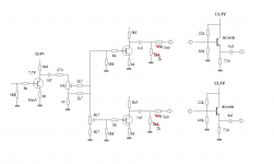
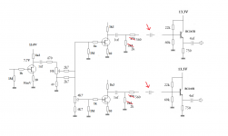
the changes
new values shown in red, and previous in black
but from what I understand, input and output impedances are not so obvious but should be calculated using bias setting
I think it was something like that

I thought the changing sound I experience would be related to load lines
Attachments
Changing sound is related to changing load line, and a few other things including the Fcutoff, harmonic distortion etc. Like choosing the capacitor, I suggest starting with a fairly neutral bias, not running the device close to max dissipation. Just focus on getting a circuit with clean signal with moderate gain and no clipping /cutoff. Once you get there, then you can play around with the biasing and load lines. It doesn't take much change in values to really change that, when you are working with13V supply with 2 gain stages. Hope your having fun.
Like choosing the capacitor, I suggest starting with a fairly neutral bias, not running the device close to max dissipation. Just focus on getting a circuit with clean signal with moderate gain and no clipping /cutoff. Once you get there, then you can play around with the biasing and load lines. It doesn't take much change in values to really change that, when you are working with13V supply with 2 gain stages. Hope your having fun.Hope your having fun.
when it works, absolutely
and Im satisfied with the buffer now
or at least it will do for experimenting
time to fool around with some tone controls
Tin,
you have repeated the same biasing mistake you had originally.
I told you to use DC blocking capacitors. You continue to ignore this.
As a result you have the 2k of the previous stage and any other parasitic resistance loading the input of the BJT buffer. This completely upsets the biasing of the buffer.
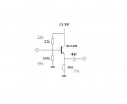
You have either 100k//2k//? in the post541 layout
and
you have 60k//2k//? in the post543 layout
as the effective lower resistor in the biasing string.
This gives the buffer an input impedance ~ 22k//2k//100k/? (about Zin = 1k8). Is your previous stage designed to drive this load? 1uF into 1k8 gives F-3dB ~ 88Hz
You must DC block both sides of the buffer to get consistent results from the circuit.
you have repeated the same biasing mistake you had originally.
I told you to use DC blocking capacitors. You continue to ignore this.
As a result you have the 2k of the previous stage and any other parasitic resistance loading the input of the BJT buffer. This completely upsets the biasing of the buffer.
You have either 100k//2k//? in the post541 layout
and
you have 60k//2k//? in the post543 layout
as the effective lower resistor in the biasing string.
This gives the buffer an input impedance ~ 22k//2k//100k/? (about Zin = 1k8). Is your previous stage designed to drive this load? 1uF into 1k8 gives F-3dB ~ 88Hz
You must DC block both sides of the buffer to get consistent results from the circuit.
Last edited:
Hi Andrew, thanks for pointing out the F-3dB calc, and at 88 Hz is cutting down the fundamentals thoughout the open string range of a standard tuned bass, and the Low E string would be cut about 6 dB. Not necessarily a bad thing for bright sound, but as you said, the input Z on the buffer is too just too low, should be at least 10 K or more. Normally a bass preamp stage should pass as much bandwidth as possible (F- 3db around 5 to 10 Hz) and use a tone stack to do it's job. DC Blocking a must here.
Have fun
Have fun
It is not funny.
We are here trying to help, but you ignore what is being said.
If something is confusing, then ask another question.
We are expending TIME to help you.
Would you rather that all those answering posts were not made and we left you with all your posts alone while you talk to yourself?
We are here trying to help, but you ignore what is being said.
If something is confusing, then ask another question.
We are expending TIME to help you.
Would you rather that all those answering posts were not made and we left you with all your posts alone while you talk to yourself?
if you remove the resistors completely then the cap on the output of the preceding stage acts as your DC block.
You can keep the series resistor as a base stopper but a base stopper should be attached to the base, not the output of the FET.
If the two stages were connected with a removable interconnect then adding a grounding resistor to take any leakage past the DC blocker is good practice. This grounding resistor (at both ends of the interconnected equipment) can usually be >1M
...but you chose to ignore his comment.
no, I made many changes after that .... and many you havent seen or heard about
man, you make feel like Im a dog
Dear Tinitus, you are very confused, becuse you are mixing 2 very different amplifier stages and considering them the same (which they are not):
1) *that* FET stage is self biased (or "cathode biased" to be more precise) and it's gate needs to be at 0V or Ground potential, so no input cap needed.
2) bipolar transistors need forward bias at the base, in that case you are "artificially" feeding it around, say, 8V DC, so you **need** to DC isolate from the previous stage or your calculations will be way off.
3) you do use a 1uF output cap after the FET stage (fine) ... but you mess with that by adding the unnecessary resistors after it.
Just pull them and you'll be fine.
Just pull them and you'll be fine.
will try that...thank you, sir
ehh...any chance the jfet stage is a current drive curcuit
I think the big man once said that 'might' happen, given certain circumstances
btw, input and output impedance isnt just a simple matter of looking at a few resistors in paralel, is it ?
I think I saw a bit more complicated calcuation the other day
anyway, I got the new att pots today...and that funny chickenhead knob
found another effort explaning input output impedance
hope its ok to post here
http://www.pdx.edu/nanogroup/sites/www.pdx.edu.nanogroup/files/2013_Input_output_impedance_9.pdf
http://www.physics.ohio-state.edu/~gan/teaching/summer04/Lec6.pdf
http://people.seas.harvard.edu/~jones/es154/lectures/lecture_3/bjt_amps/bjt_amps.html
hope its ok to post here
http://www.pdx.edu/nanogroup/sites/www.pdx.edu.nanogroup/files/2013_Input_output_impedance_9.pdf
http://www.physics.ohio-state.edu/~gan/teaching/summer04/Lec6.pdf
http://people.seas.harvard.edu/~jones/es154/lectures/lecture_3/bjt_amps/bjt_amps.html
and this 'statement'
There are two "tricks" to answering those questions with transistor amplifiers.
The first trick is to understand that the current-transfer ratio (hFE) of a transistor effectivly multiplies the resistance at its emitter. So, to find the impedance looking into the base, you calculate the effective resistance at its emitter, multiply this by hFE, and then add the internal base resistance.
The second trick is to realize that the result of the calculation above is typically orders of magnitude larger than the other resistances connected to the base of the transistor and can therefore be ignored.In other words, the input impedance of a transistor amplifier is usually very close to the impedance of its bias network alone. Indeed, bias networks are very often designed so that this is the case.
The output impedance is a question of how much the output voltage changes with output current: ΔV/ΔI. The transistor itself is essentially a current source, and whatever current it is passing is shared between the various resistances connected to the emitter. Therefore, the output impedance is equal to the net emitter resistance, not including the resistance of the external load.
In other words, the input impedance of a transistor amplifier is usually very close to the impedance of its bias network alone.
Big blanket statement which *sometimes* is true, many times is not, by a *long* margin.
I suggest you start flying low and go step by step; otherwise you'll very often find blanket statements such as the one you quote, which should contain the word "if" many times, then confusing you because some other "authority" says what *looks* like the opposite ..... and you can't tell them apart because you lack the fine detail of what's happening.
Maybe they don't bother to explicitly mention them because they think you "already know" them and don't want to repeat themselves .... but you probably didn't read 3 pages (or 2 chapters or another book) earlier where they explained *why*.
- Status
- This old topic is closed. If you want to reopen this topic, contact a moderator using the "Report Post" button.
- Home
- Live Sound
- Instruments and Amps
- Switchable Hi-Z input impedance, how ?