MOSFET pass device issues
Part of my intent in posting the cascode information was to underscore how simple a clean source can actually be. 2 DN2540's and a resistor, can work from Vout or Vin.
I'll chime in here, on MOSFET pass devices...
Pro: Ultra low DC drive, wide range of parts, complements available.
Con: Very high Cin, high threshold vs. BJT means higher dropout, enhancement parts need help for turnon.
For the topology as used in a superreg, MOSFETs may need some work to adapt, i.e., won't drop in directly. Can be made to work, but I personally haven't done it, so I can't advise beyond the above.
But, if you are making *only* a POS type reg., a DN2540 will possibly work with relatively little effort, since it is a depletion mode part.")
Good luck, and keep us posted!
Post 358
Post 370
I'm glad we have violent agreement on how to get a good Vref when driven by Vin and we can split hairs over whether the cost of a few extra parts is worth it.
Presumably in a MOSFET pass device setup rather than BJT setting Vref from Vin becomes a necessity? I also seem to be tying myself in knots as to how to power the op-amp in this situation. Again, is one forced to power from Vin? How important is a stable supply for the op amp?
Part of my intent in posting the cascode information was to underscore how simple a clean source can actually be. 2 DN2540's and a resistor, can work from Vout or Vin.
I'll chime in here, on MOSFET pass devices...
Pro: Ultra low DC drive, wide range of parts, complements available.
Con: Very high Cin, high threshold vs. BJT means higher dropout, enhancement parts need help for turnon.
For the topology as used in a superreg, MOSFETs may need some work to adapt, i.e., won't drop in directly. Can be made to work, but I personally haven't done it, so I can't advise beyond the above.
But, if you are making *only* a POS type reg., a DN2540 will possibly work with relatively little effort, since it is a depletion mode part.
Good luck, and keep us posted!
Last edited:
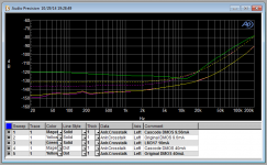
Zeners are optimally biased (for noise) around 10mA -- I used several varieties of bypass (1uF) caps and am not seeing any benefit to the cascode at this level of current demand if just used for a voltage reference. (The '2540's are matched @44mS). I threw an LM317 in there for good measure.
When the current demand is ramped to 40mA there is a significant betterment of the cascode:
When the current demand is ramped to 40mA there is a significant betterment of the cascode:
Attachments
Last edited:
Question what does the noise floor look like in this graph (reference level) please.Zeners are optimally biased (for noise) around 10mA -- I used several varieties of bypass (1uF) caps and am not seeing any benefit to the cascode at this level of current demand if just used for a voltage reference. (The '2540's are matched @44mS). I threw an LM317 in there for good measure.
When the current demand is ramped to 40mA there is a significant betterment of the cascode:
Last edited:
Question what does the noise floor look like in this graph (reference level) please.
The noise floor of the SYS2722 is probably 6dB lower than Walt's unit.
I am using an injector from Omicron Labs as I can't get to the source I used in the LA article. (Those Austrian's know how to make good, albeit expensive stuff!)
The graph is to show the relative merits which are profound at higher current levels.
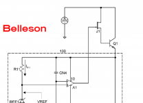
Belleson and SuperTeddy use a high-IDSS JFET (whose pinchoff voltage is quite a large negative number) in a Darlington-lookalike configuration, driving the base of a BJT series pass transistor. Voila, high input impedance, low input capacitance, control voltage below the supply rail, and low input-to-output dropout voltage. Belleson's circuit even discards the level shifting zener and merely drives the JFET's gate straight from the opamp output pin.
Difficulty: it is not easy to find high-IDSS Pchannel JFETs to build negative regulators.
Another thing you could do, is carefully study the datasheets of the ridiculously low Rds_on, automotive MOSFETs. Some of them have dIds/dVgs greater than BJTs (Jan Didden's holy grail: higher gm). Yes they exist. The good news is, you can get them with relatively low capacitance and incredibly high fT, in both Pchannel and Nchannel. The bad news is, you have to search for them, yourself. The ones with the best datasheets might not be sold on your continent. And they may have a large dropout voltage: (Vin-Vout) might be as big as 3 or 3.5 volts. You could build a charge pumped Vgg supply to ameliorate this; or if you're designing a low-wattage power supply, you could just buy a transformer with one click higher secondary voltage. The vendor that I buy 50VA R-core transformers from, charges the same price for a 12VAC secondary as for an 18VAC secondary. Doubtful that your preamp or DAC is going to need anywhere near 50 volt-amps.
Last edited:
But, if you are making *only* a POS type reg., a DN2540 will possibly work with relatively little effort, since it is a depletion mode part.
Good luck, and keep us posted!
Hi. I'm tinkering with far higher current needs which is why I'm looking at FETs. Nonetheless, it is very instructive to understand your super regulator better and the preceding discussion here (all the way back to around post #177 or so) re FET vs BJT. I still have a lot to learn.
Another thing you could do, is carefully study the datasheets of the ridiculously low Rds_on, automotive MOSFETs. Some of them have dIds/dVgs greater than BJTs (Jan Didden's holy grail: higher gm). Yes they exist. The good news is, you can get them with relatively low capacitance and incredibly high fT, in both Pchannel and Nchannel. The bad news is, you have to search for them, yourself.
I have no problem doing the grunt work and thanks for guiding as to what to look for. At the moment I'm trying to get the basic topology modeled correctly as currently the output isn't making any sense whatsoever. I will persevere.
I should clarify my last statement. Modelling with an LTC1150 or LT1797 op amp all looks sensible. However, if I download the Spice model for the AD797A, create a new symbol and drop that into the model things don't look right at all. (I've checked the net list order several times.)
I haven't really experimented with a FET as a pass device. The way I see it, the much lower gain/transconductance of a FET wrt a bipolar will result in lower measured performance.
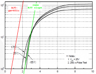
Here's another MOSFET, different from the one in (post #194). I've drawn the (gm = Ic/(kT/q)) curve of a BJT, on top of a MOSFET datasheet's Ids-Vgs plot. At +25C and -55C the MOSFET has steeper slope, i.e., greater gm. However this is only true at low currents (Ids < 10 amps). After that, the effects of rds_on start to take over.
_
Attachments
Remember that a bipolar transistor has gm = 40*Ic at room temperature. gm is a function of the collector current.
A MOSFET's gm is also a function of its drain current.
To compare a MOSFET's gm to a bipolar's gm, you need to operate both devices at the same current. One easy way to carry out the comparison, is to compute the MOSFET's (gm/Ids) ratio. If the ratio is greater than 40, the MOSFET's gm is superior to a bipolar's gm... at this current level.
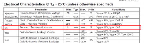
Here is an example from a MOSFET datasheet. The quoted transconductance is 91 siemens at 104 amperes; the ratio is (91/104) = 0.87, not nearly as good as a bipolar. However if we look at the curves on subsequent pages of the same datasheet, we see that the slope of Ids vs Vgs might, just might, exceed the gm slope of a bipolar ... at low current (below 10 amperes). This requires eyeball extrapolation and so the results should be considered illustrative rather than definitive.
The datasheet gfs@Ids is only helpful if it is quoted at low currents.
_
A MOSFET's gm is also a function of its drain current.
To compare a MOSFET's gm to a bipolar's gm, you need to operate both devices at the same current. One easy way to carry out the comparison, is to compute the MOSFET's (gm/Ids) ratio. If the ratio is greater than 40, the MOSFET's gm is superior to a bipolar's gm... at this current level.
Here is an example from a MOSFET datasheet. The quoted transconductance is 91 siemens at 104 amperes; the ratio is (91/104) = 0.87, not nearly as good as a bipolar. However if we look at the curves on subsequent pages of the same datasheet, we see that the slope of Ids vs Vgs might, just might, exceed the gm slope of a bipolar ... at low current (below 10 amperes). This requires eyeball extrapolation and so the results should be considered illustrative rather than definitive.
The datasheet gfs@Ids is only helpful if it is quoted at low currents.
_
Attachments
Last edited:
Con: Very high Cin
What is the trade-off with (gate?) capacitance?
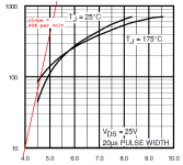
While I was playing around today trying to get this reg model to work I was using the IRFP4368, if only because it has very high gm (as quoted), low Rds(on), a convenient, isolated package and a Spice model. I note that its Ids vs Vgs curve remains very steep for a considerable period and would seem to easily meet the delta Ids / V > 40 for a considerable current range. While not the cheapest FET, they are readily available from Mouser UK.
One other question: a low pass filter filter for Vref helps a lot but doesn't for Vs for the op amp. Why not?
Last edited:
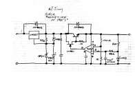
JFET_Drive_Regulator~1980
1) In MOSFETs, the Cin can be huge, hundreds of pF, or even a nF. To control the current, this cap must be driven. The capacitance is non-linear, so this creates potential if not real IM products.
The attached sch "JFET_Drive_Reg_~1980" shows (in principle) how a high Vgs(off) N-channel JFET (-4 to -10V for a 2N/PN4391) can be used to control an NPN bipolar. I don't know if I ever built this exact setup, this was a "thinking process" sketch, from sometime in the 1980's. (Don't be hasty to critique the op amp choice, or other details).
But, this scheme of control devices results in a lower Cin for the NPN, vis-a-vis a MOSFET. The FET/bipolar combo would be a functional equivalent of a depletion mode power FET (such as the DN2540). But here one can tweak performance by choice of FET/NPN.
A pre-reg is suggested by the use of the LM317, as Vgs of the FET will otherwise vary with the unregulated Vin.
2) I'm not sure what you are asking in this point, SGK. helps what?
1) What is the trade-off with (gate?) capacitance?
While I was playing around today trying to get this reg model to work I was using the IRFP4368, if only because it has very high gm (as quoted), low Rds(on), a convenient, isolated package and a Spice model. I note that its Ids vs Vgs curve remains very steep for a considerable period and would seem to easily meet the delta Ids / V > 40 for a considerable current range. While not the cheapest FET, they are readily available from Mouser UK.
2) One other question: a low pass filter filter for Vref helps a lot but doesn't for Vs for the op amp. Why not?
1) In MOSFETs, the Cin can be huge, hundreds of pF, or even a nF. To control the current, this cap must be driven. The capacitance is non-linear, so this creates potential if not real IM products.
The attached sch "JFET_Drive_Reg_~1980" shows (in principle) how a high Vgs(off) N-channel JFET (-4 to -10V for a 2N/PN4391) can be used to control an NPN bipolar. I don't know if I ever built this exact setup, this was a "thinking process" sketch, from sometime in the 1980's. (Don't be hasty to critique the op amp choice, or other details).
But, this scheme of control devices results in a lower Cin for the NPN, vis-a-vis a MOSFET. The FET/bipolar combo would be a functional equivalent of a depletion mode power FET (such as the DN2540). But here one can tweak performance by choice of FET/NPN.
A pre-reg is suggested by the use of the LM317, as Vgs of the FET will otherwise vary with the unregulated Vin.
2) I'm not sure what you are asking in this point, SGK. helps what?
Attachments
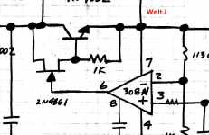
Hi Walt, that's the same JFET-BJT compound follower circuit also used in the SuperTeddy and Belleson regulators, which Jan was talking about in (post #386) above. Neither the SuperTeddy nor the Belleson finished among the top of the pack in John Walton's voltage regulator testing (Linear Audio vol.4), a finding which Jan suggests "might be instructive" when considering the compound follower circuit.
Attachments
2) I'm not sure what you are asking in this point, SGK. helps what?
Thx. By this I meant that a low pass filter is deployed for Vref. If I try to add similar to V+ powering the op amp (assuming the op amp is powered from Vin) I get much worse noise rejection.
Thx. By this I meant that a low pass filter is deployed for Vref. If I try to add similar to V+ powering the op amp (assuming the op amp is powered from Vin) I get much worse noise rejection.
Well... I'm not sure why that might be so. But running the OA from Vout sure takes care of lots of problems.
Hi Walt, that's the same JFET-BJT compound follower circuit also used in the SuperTeddy and Belleson regulators, which Jan was talking about in (post #386) above. Neither the SuperTeddy nor the Belleson finished among the top of the pack in John Walton's voltage regulator testing (Linear Audio vol.4), a finding which Jan suggests "might be instructive" when considering the compound follower circuit.
Interesting point, indeed. I don't know about sonic merits/faults of the JFET/BJT combo, but I do know it can degrade stability. It helps to run the JFET a bit warm (several mA; the 1k B-E R as shown is not necessarily a good value in that regard). Also a feedback cap back to the OA (-) input may help.
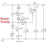
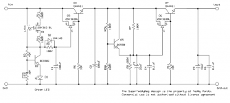
I note that the SuperTeddy isn't a real regulator, just a follower buffering an RC filter..
Last edited:
I deleted the second half of the SuperTeddy circuit, to reduce clutter and to better draw attention to the compound follower. Below is the full and complete schematic from Teddy Pardo's DIY page.I note that the SuperTeddy isn't a real regulator, just a follower buffering an RC filter..
Teddy considers the first stage to be a voltage regulator and the second stage to be a lowpass filter. He reasons that Q2 works just like a VBE multiplier. The voltage at the base of Q2 (VgreenLed + Vbe2) is multiplied by R2/R3 to get the collector voltage. JFET Q1 provides approx. constant current, so the LED current is constant and Q2's base current is constant (he reasons), therefore VgreenLed is constant and Vbe2 is constant. This means (R2/R3) times (VgreenLED + Vbe2) is a constant voltage. It is in effect a "shunt regulator" fed from a constant current source. It presents a fixed, reference voltage to the Q3-Q4 compound follower.
The second stage is just an RC filter (R7, R8, C3) driving another compound follower Q6-Q7. Transistor Q5 is merely a helper device that accelerates startup and then gets out of the way. So is diode D5.
Personally I think it might be preferable to interchange the order of the two stages: buffered filter then regulator. But then I also think it would be preferable to include each follower within a high gain NFB loop, which seems to be the precise opposite of the entire SuperTeddy philosophy.
Interestingly, he runs the JFETs at about 3mA each, via R6 and R11 (for Vout = 30V).
Attachments
Last edited:
I note that the SuperTeddy isn't a real regulator, just a follower buffering an RC filter..
You beat me to it.
- Home
- The diyAudio Store
- Super Regulator