Folks,
Maybe I'll explain a little more the logic behind the various design choices.
One of my main requirements was the circuit would have to fit the existing PCB and reuse as much of the existing amplifier as possible. The existing Amplifier
The second requirement was that what I perceive as design weaknesses are addressed. For example experience tells me that too much negative feedback produces a sound quality I dislike.
Generally the concept is quite similar to the APT-1 Poweramp, however many bipolars are replaced by by Fets.
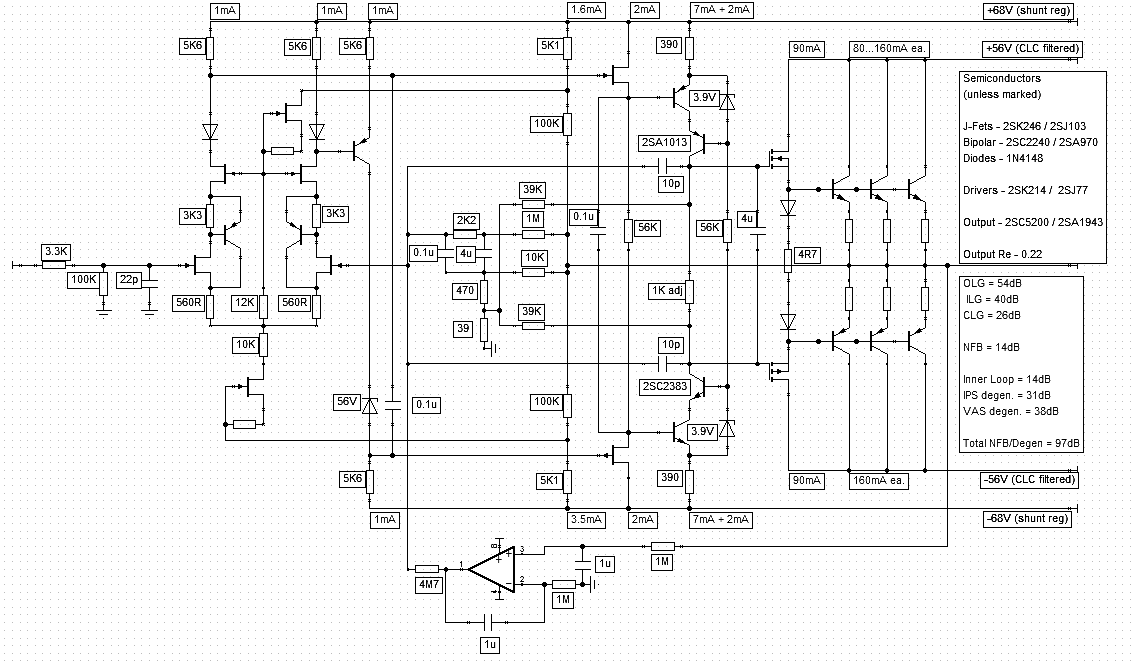
Input Stage
The input stage uses a compound feedback pair simply to exploit the better linearity of the degenerated bipolar transistor and to offload much of the dissipation (and dissipation variation) to the bipolar transistor. As the FET has a very high FT and low capacitance, the bipolar transistors determine the bandwidth on the input stage. The input Fet's are operated near the Zero tempco point (will likely tune some more for operation precisely at zero Tempco).
The cascode is referenced to the common mode voltage of the input stage, so the voltage across the input stage shows by far less variation than it would if the cascode was referenced to ground. The current sources that set tail current and the one biasing the cascode are both J-Fet based with impedances of around 100K. However, they are bootstrapped (fine tuning still needed) so the voltage across them does not vary with signal, so the apparent impedance of them will by far greater.
Thus the input stage has minimised all common mode problems. This will not easily show up in classic THD & N Analysis, however listen to the same Op-Amp with an input stage that has not been aggressively protected from common mode problems in non-inverting and inverting mode and the import becomes clear. Equally, the import of the linearity of the IPS can not be over-emphasised. This is where Feedback and Signal are "mixed" and any non-linearity in this process is not reduced by the looped NFB.
In order to generate the signal to drive the push-pull VAS one of the two opposite polarity signals from the input differential is "mirrored" down to the negative rail, using a heavily degenerated simple current mirror. If a mirror is sufficiently degenerated and loaded by a modest load impedance the action of this very simple circuit is as near to perfect as need be. Overall gain is around 5 for the differential frontend with the single ended output, with a very large amount of degeneration applied.
VAS Buffer and VAS
A little trick is the capacitor that links the two signals driving the VAS. In theory both signals should be identical, so if the circuit is perfectly balanced the capacitor has no effect. If there are differences this capacitor will "zero" them. It also ensures that the different input capacitances of the N and J-Fet buffer cause no asymmetric capacitive loading.
The total input capacitance of the J-Fet buffer is around 6pF, the output impedance of the input stage comes in at around 2.8K, for an F3 of around 10MHz.
The J-Fet buffer as far as AC is concerned is basically a straightforward complementary "JC" J-Fet buffer. For DC the inputs and outputs are shifted as required. However as the two sources are linked the VAS Base's are again at the same potential for AC.
So any asymmetry from the various non-ideal transistor properties that are referred back to the Base's are equalised. Another noteworthy effect, the J-Fets at the operating current have a similar negative tempco as the negative tempco of the bipolar transistors so they net off very much similar to the use of "halve-diamond" bipolar buffer, overall the Tempco of the VAS Current should be slightly negative (lowering with rising temperature). I will try to trim this as close to zero as possible (by changing the common source resistor of the buffer).
The output impedance of the buffer is around 200 ohm, while the degenerated VAS has around 60K low frequency input impedance. The VAS is cascoded, which reduces the miller capacitance and early effect of the VAS further, so the 60K input impedance should hold up to quite high frequencies. So unlike in most amplifiers, the VAS clearly operates voltage driven, not as current driven transimpedance stage. The benefits for linearity should be obvious.
The VAS has a gain of 10, set by it's loading resistors. The output impedance of the VAS is around 20KOhm. The VAS can swing a maximum of 14mA peak, to swing 50V Peak only around 18% of the available swing are needed. The "small lateral" Fet drivers in the output stage present around 10-12pF load to the VAS, so theoretical Slew Rate at this node is off the charts and theoretical bandwith with the compensation applied is 265KHz (open Loop). The limit for slew rate will be with the output transistors.
Paradoxically, at least in Tina-Ti removing this load does not lower THD(50k) but increases the odd order distortion (and thus THD) appreciably even though loop gain is increased over 20dB!?
Output Stage
The Output stage combines the "small" Lateral Mosfet Drivers (operating at appx. 80...90mA) with a bipolar output stage operating in Class AB, final bias will be tested in the actual article, 26mV are used in simulation. Under these conditions the lateral Mosfets have a slightly larger positive tempco than the negative tempco of the output transistors.
So if all of them are mounted on the same heatsink and the rest of the amplifier is stable (which as you may have noticed from earlier sections it is) there is no need for a VBE Multiplier, the output stage stabilises it's quiescent current itself. The "small laterals" have a large enough source resistance (around 10 ohm each) that base-stoppers can be omitted, negative impedance oscillation is no longer possible.
The diodes in the source resistor chain reduce the resistance in the drivers source circuit, so any charge can be more effectively evacuated from switched off halve of the output.
It may seem counter-intuitive, but a sufficiently large common (to both halves of the output stage) resistance to stop negative impedance oscillation introduces less increase in crossover distortion than individual base stoppers. Total open loop output impedance is around 0.15 Ohm.
Under ideal conditions using an EF3 Stage with a "diamond transistor" driver fully thermally compensated on it's own heatsink and with a single pair VBE compensation can perform marginally better in terms of input capacitance with input impedance past good or bad and similar thermal behaviour, however circuit complexity is increased significantly for notional differences. In principle the "diamond driver" could also be made using the same J-Fets as buffer the VAS and some suitable Driver transistors for a new design.
For a "minimal change retrofit" this complexity makes it a poor option, but it deserves serious consideration for a new design.
Complete Circuit
Anyway, under pure open loop conditions the open loop gain is around 54dB with -3dB points at 16Hz and 120KHz, I suspect the real devices would improve this further towards the theoretical 260Khz or so. Tina-Ti predicts around 0.16% THD(1K) and 0.46% THD(20K) for the open loop amplifier at 26V into 8 Ohm.
Closing the inner loop applies around 12dB local looped feedback to the VAS, extending the -3dB bandwidth to 5Hz-500KHz. This according to Tina-Ti gives 0.1% THD(1K) and 0.18% THD(20K). This indicates that the VAS is still a significant source of distortion, despite all the measures applied to linearise it.
Closing the outer loop now gives predictable performance. Closed loop gain is a touch below the 26dB target, due to using standard values. The HF bandwidth is not extended as the compensation remains present so 0.5MHz -3dB it remains, at the low end -3dB shifts to 1Hz. THD (1K) becomes 0.017% and THD(20K) becomes 0.045% for 26V into 8Ohm. Output impedance looks like around 25mOhm (aka a dumping factor of 320).
I suspect that much of the THD rise at higher frequencies comes in part from the Fet Models, namely IRF610/9610 which still have well over three times the capacitance of the laterals and much greater voltage dependence of the capacitances (making them in fact pee-poor choices as drivers) and the fact that model output transistors (TIP33/34) are rather slow devices.
Time to shift to LT-Spice I think.
Ciao T
I made some changes and got fed up with working in the "pen, paper, slipstick" domain.
....
Maybe I'll explain a little more the logic behind the various design choices.
One of my main requirements was the circuit would have to fit the existing PCB and reuse as much of the existing amplifier as possible. The existing Amplifier
The second requirement was that what I perceive as design weaknesses are addressed. For example experience tells me that too much negative feedback produces a sound quality I dislike.
Generally the concept is quite similar to the APT-1 Poweramp, however many bipolars are replaced by by Fets.
Input Stage
The input stage uses a compound feedback pair simply to exploit the better linearity of the degenerated bipolar transistor and to offload much of the dissipation (and dissipation variation) to the bipolar transistor. As the FET has a very high FT and low capacitance, the bipolar transistors determine the bandwidth on the input stage. The input Fet's are operated near the Zero tempco point (will likely tune some more for operation precisely at zero Tempco).
The cascode is referenced to the common mode voltage of the input stage, so the voltage across the input stage shows by far less variation than it would if the cascode was referenced to ground. The current sources that set tail current and the one biasing the cascode are both J-Fet based with impedances of around 100K. However, they are bootstrapped (fine tuning still needed) so the voltage across them does not vary with signal, so the apparent impedance of them will by far greater.
Thus the input stage has minimised all common mode problems. This will not easily show up in classic THD & N Analysis, however listen to the same Op-Amp with an input stage that has not been aggressively protected from common mode problems in non-inverting and inverting mode and the import becomes clear. Equally, the import of the linearity of the IPS can not be over-emphasised. This is where Feedback and Signal are "mixed" and any non-linearity in this process is not reduced by the looped NFB.
In order to generate the signal to drive the push-pull VAS one of the two opposite polarity signals from the input differential is "mirrored" down to the negative rail, using a heavily degenerated simple current mirror. If a mirror is sufficiently degenerated and loaded by a modest load impedance the action of this very simple circuit is as near to perfect as need be. Overall gain is around 5 for the differential frontend with the single ended output, with a very large amount of degeneration applied.
VAS Buffer and VAS
A little trick is the capacitor that links the two signals driving the VAS. In theory both signals should be identical, so if the circuit is perfectly balanced the capacitor has no effect. If there are differences this capacitor will "zero" them. It also ensures that the different input capacitances of the N and J-Fet buffer cause no asymmetric capacitive loading.
The total input capacitance of the J-Fet buffer is around 6pF, the output impedance of the input stage comes in at around 2.8K, for an F3 of around 10MHz.
The J-Fet buffer as far as AC is concerned is basically a straightforward complementary "JC" J-Fet buffer. For DC the inputs and outputs are shifted as required. However as the two sources are linked the VAS Base's are again at the same potential for AC.
So any asymmetry from the various non-ideal transistor properties that are referred back to the Base's are equalised. Another noteworthy effect, the J-Fets at the operating current have a similar negative tempco as the negative tempco of the bipolar transistors so they net off very much similar to the use of "halve-diamond" bipolar buffer, overall the Tempco of the VAS Current should be slightly negative (lowering with rising temperature). I will try to trim this as close to zero as possible (by changing the common source resistor of the buffer).
The output impedance of the buffer is around 200 ohm, while the degenerated VAS has around 60K low frequency input impedance. The VAS is cascoded, which reduces the miller capacitance and early effect of the VAS further, so the 60K input impedance should hold up to quite high frequencies. So unlike in most amplifiers, the VAS clearly operates voltage driven, not as current driven transimpedance stage. The benefits for linearity should be obvious.
The VAS has a gain of 10, set by it's loading resistors. The output impedance of the VAS is around 20KOhm. The VAS can swing a maximum of 14mA peak, to swing 50V Peak only around 18% of the available swing are needed. The "small lateral" Fet drivers in the output stage present around 10-12pF load to the VAS, so theoretical Slew Rate at this node is off the charts and theoretical bandwith with the compensation applied is 265KHz (open Loop). The limit for slew rate will be with the output transistors.
Paradoxically, at least in Tina-Ti removing this load does not lower THD(50k) but increases the odd order distortion (and thus THD) appreciably even though loop gain is increased over 20dB!?
Output Stage
The Output stage combines the "small" Lateral Mosfet Drivers (operating at appx. 80...90mA) with a bipolar output stage operating in Class AB, final bias will be tested in the actual article, 26mV are used in simulation. Under these conditions the lateral Mosfets have a slightly larger positive tempco than the negative tempco of the output transistors.
So if all of them are mounted on the same heatsink and the rest of the amplifier is stable (which as you may have noticed from earlier sections it is) there is no need for a VBE Multiplier, the output stage stabilises it's quiescent current itself. The "small laterals" have a large enough source resistance (around 10 ohm each) that base-stoppers can be omitted, negative impedance oscillation is no longer possible.
The diodes in the source resistor chain reduce the resistance in the drivers source circuit, so any charge can be more effectively evacuated from switched off halve of the output.
It may seem counter-intuitive, but a sufficiently large common (to both halves of the output stage) resistance to stop negative impedance oscillation introduces less increase in crossover distortion than individual base stoppers. Total open loop output impedance is around 0.15 Ohm.
Under ideal conditions using an EF3 Stage with a "diamond transistor" driver fully thermally compensated on it's own heatsink and with a single pair VBE compensation can perform marginally better in terms of input capacitance with input impedance past good or bad and similar thermal behaviour, however circuit complexity is increased significantly for notional differences. In principle the "diamond driver" could also be made using the same J-Fets as buffer the VAS and some suitable Driver transistors for a new design.
For a "minimal change retrofit" this complexity makes it a poor option, but it deserves serious consideration for a new design.
Complete Circuit
Anyway, under pure open loop conditions the open loop gain is around 54dB with -3dB points at 16Hz and 120KHz, I suspect the real devices would improve this further towards the theoretical 260Khz or so. Tina-Ti predicts around 0.16% THD(1K) and 0.46% THD(20K) for the open loop amplifier at 26V into 8 Ohm.
Closing the inner loop applies around 12dB local looped feedback to the VAS, extending the -3dB bandwidth to 5Hz-500KHz. This according to Tina-Ti gives 0.1% THD(1K) and 0.18% THD(20K). This indicates that the VAS is still a significant source of distortion, despite all the measures applied to linearise it.
Closing the outer loop now gives predictable performance. Closed loop gain is a touch below the 26dB target, due to using standard values. The HF bandwidth is not extended as the compensation remains present so 0.5MHz -3dB it remains, at the low end -3dB shifts to 1Hz. THD (1K) becomes 0.017% and THD(20K) becomes 0.045% for 26V into 8Ohm. Output impedance looks like around 25mOhm (aka a dumping factor of 320).
I suspect that much of the THD rise at higher frequencies comes in part from the Fet Models, namely IRF610/9610 which still have well over three times the capacitance of the laterals and much greater voltage dependence of the capacitances (making them in fact pee-poor choices as drivers) and the fact that model output transistors (TIP33/34) are rather slow devices.
Time to shift to LT-Spice I think.
Ciao T
Hi,
Because in my case I want to re-use the output stage PCB and Heatsink of an existing Amp, which happens to have three pairs. Other than that I agree, adding more output devices would be a good choice.
Ciao T
why didn't you add another pair (or two) of the output devices?
Because in my case I want to re-use the output stage PCB and Heatsink of an existing Amp, which happens to have three pairs. Other than that I agree, adding more output devices would be a good choice.
Ciao T
Hi,
The best to imagine the servo is to consider the capacitors first as resistors. In this case an inverting Op-Amp is in the Feedback loop of the servo and thus the servo is non-inverting. Any Voltage on the output of the inverting main amp is amplified by the Servo Op-Amp and then re-injected into the inverting input of the Op-Amp. This will oppose any change of the output voltage of the main amplifier.
Now we add the capacitors back.
Above a certain AC frequency, the capacitors will have a very low impedance, yet the DC resistance is basically infinity. So for DC the circuit of the amplifier has a gain of 1. For AC the gain is around 20.
As the input section does not use monolithic pairs and the input fets (as well as the VAS Buffers and driver laterals) are not necessarily matched, we still get potentially quite a bit of offset, especially given the amplifiers relatively low DC Gain (a little over 50dB). Hence the servo is added to null out this offset.
The fact that we inject the servo output through 4.7MOhm into the inverting input where the impedance to ground is around 470 Ohm (assuming the capacitors in the main amplifiers feedback network are shorted) means the output from the servo is attenuated by around 80dB. Another way to view this is to say that the signal from the servo passes through a first order 0.01Hz lowpass, with a Zero at around 16Hz, thus giving a PI regulator behaviour.
The servo itself is differential and has 0.16Hz cutoff. It means at 0.16Hz the gain of the circuit is only 3dB above unity and the input filter will attenuatre 3dB. So at 16Hz the servo itself will filter any signal from the main Amp by 40dB, so the AC on the servo output for a full 50V peak swing becomes 0.5V. This as remarked is then attenuated a further 80dB due to the way the servo signal is injected into the inverting input.
Meanwhile DC will be amplified by the full DC gain of our Op-Amp (OPA-627), that is by 120dB. The DC Gain for the injected signal is around 0.2, we we retain over 100dB DC Loop gain. This gain of the servo Amp charges the capacitor in the Servo Amp feedback progressively, while shifting the output of the Op-Amp, which in turn charges the capacitors in the Amplifiers feedback loop.
This in turn causes the DC voltage appearing on the output of the Amplifier to be reduced. Eventually the system will reach an equilibrium. As we are dealing with a total 2nd Order filter in a loop we have potential for instability, so I will have to do a sim for that to check.
Ciao T
Hi Thorsten,
Thanks for this explanation. Simming will indeed show if you need to tone down the gain of the opamp and lower the value of the resistor back into the feedback loop. My gut feeling is that it would be more stable to have all the low pass filtering done in one place, that is before the opamp, and not distributed in part before, and part after the opamp output in the way it is connected to the feedback loop. Please let us know when you come round simming it.
vac
I have not interest to improve what you call global linearity beyond certain minimal requirements. There is no evidence that doing so provides any tangible benefits.
Once you understand that you may be able to focus on things that actually matter.
I would call stability a minimal requirement and a parameter that
really matter...or is it ??..
As presented this amp will oscillate.
Well, The DH-120 project is playing on real speakers, stable, and for sure, quieter. It passes my Segovia "metallic string fault" test. I won't know about the wife test for a while. Power supply upgrades, wiring changes, outputs, correct gate stoppers for symmetrical output speed, moving the compensation so symmetrical rise and fall? One of those helped. I did not put in the TMC or switch the input CCS to FET and I left the protection diodes in.
Time to quit mucking with amps temporally and build some speakers. I have to admit, kind of hooked on the problems of amps. I am no closer to understanding why some pass the wife test and some do not, but more convinced than ever it is an interaction between the amp and the tweeter, not a fault per say of the amp. My list of things to try is a mile long. I want to get to something I can measure, point to and then know how to fix.
Time to quit mucking with amps temporally and build some speakers. I have to admit, kind of hooked on the problems of amps. I am no closer to understanding why some pass the wife test and some do not, but more convinced than ever it is an interaction between the amp and the tweeter, not a fault per say of the amp. My list of things to try is a mile long. I want to get to something I can measure, point to and then know how to fix.
Hi,
Not according to Tina-Ti, however this may be the result of using the "wrong"models. Due to the differences between real and simulated circuit I find that compensation needs to be optimised individually with the actual layout and devices.
Ciao T
I would call stability a minimal requirement and a parameter that really matter...or is it ??..
As presented this amp will oscillate.
Not according to Tina-Ti, however this may be the result of using the "wrong"models. Due to the differences between real and simulated circuit I find that compensation needs to be optimised individually with the actual layout and devices.
Ciao T
Hi Thorsten,
Thanks for this explanation. Simming will indeed show if you need to tone down the gain of the opamp and lower the value of the resistor back into the feedback loop. My gut feeling is that it would be more stable to have all the low pass filtering done in one place, that is before the opamp, and not distributed in part before, and part after the opamp output in the way it is connected to the feedback loop. Please let us know when you come round simming it.
vac
Perhaps you may find this little document useful, so I'm posting it here, just in case.
Attachments
Well, The DH-120 project is playing on real speakers, stable, and for sure, quieter. It passes my Segovia "metallic string fault" test. I won't know about the wife test for a while. Power supply upgrades, wiring changes, outputs, correct gate stoppers for symmetrical output speed, moving the compensation so symmetrical rise and fall? One of those helped. I did not put in the TMC or switch the input CCS to FET and I left the protection diodes in.
Time to quit mucking with amps temporally and build some speakers. I have to admit, kind of hooked on the problems of amps. I am no closer to understanding why some pass the wife test and some do not, but more convinced than ever it is an interaction between the amp and the tweeter, not a fault per say of the amp. My list of things to try is a mile long. I want to get to something I can measure, point to and then know how to fix.
My heartiest congratulations!
Of course, with the amount of work you put in, you could hardly fail to improve on it, but still, it always feels good when you hear somebody did it.
I think your decision to turn to loudspeakers now is a wise one. If one goes too deep into any one field, one is tempted to really overdo it (as one is swamped with new data) and possibly get lost in it (goven that it's not your everyday profession). I find it helps when you let go for a while, take a break and go do something else, and let what you have acquired in knowledge and experience simmer down and sort of mature in your head.
Then, when you come back to it, it's on a different plane of understanding. I strongly suspect your comeback to the amplifier arena will be in form of making your own, evading many of the problems you had right from the design stage.
Anyhow, way to go, Tvr!
Hi,
Not according to Tina-Ti, however this may be the result of using the "wrong"models. Due to the differences between real and simulated circuit I find that compensation needs to be optimised individually with the actual layout and devices.
Ciao T
I couldn't agree more. And it works both ways.
When I was working on the solid state versions of my headamps, I allowed space for the compensation as on the design. The simulator model was sort of iffy, maybe I'd need it, and maybe I wouldn't, clear as mud.
In the end, it turned out that I don't actually need it.
Think of it this way, Thorsten - that simulator has to ASSUME something, for example, that yopu will be using PC boards with say 30...35 microns of copper, as an industry standard. Thus it also assumes things like parasitic capacitances and so forth.
I used 70 micron PC boards (my personal standard) as I always do, and the board came out very nicely compact, but not too compact (meaning that we didn't push for still more compact at the cost of copper trace width, I like nice, wide and thick lines). Appearently, the actual parasitic capacitance was on a lower level than the simulator assumed, and the actual measured results were at worst 10% better than the simulator told me - for example, it put the higher -3 dB point at 1.2 MHz, and it actually measured 1.6 MHz. The compensation simply was not needed in real life.
However, mostly it's the other way around. The sim says say 2 pF, and you discover you actually need 3.3 pF, etc. No matter what the simulation looks like on the screen, until you have the actual, live model on your test bench, it's just a more or less educated guess.
Think of it this way, Thorsten - that simulator has to ASSUME something, for example, that yopu will be using PC boards with say 30...35 microns of copper, as an industry standard. Thus it also assumes things like parasitic capacitances and so forth.
Perhaps you are using more sophisticated simulators, but my programs make no assumptions about such layout parasitics like trace resistance and capacitances. These have to be incorporated explicitly.
Perhaps you may find this little document useful, so I'm posting it here, just in case.
Thanks DVV, very useful.
Thanks DVV, very useful.
My pleasure.
Perhaps you are using more sophisticated simulators, but my programs make no assumptions about such layout parasitics like trace resistance and capacitances. These have to be incorporated explicitly.
Multism Professional 10.3, the only program I have which I did not buy. I simply couldn't afford it, it costs something like $7,000 or so.
It has its problems, among them a criminally low transistor database (but it does let me make my own SPICE model definitions from a say Data Sheet), but it has not lied to me ever, not once, over the last 6 years (of using it and its predecessors). If anything, it's a little pessimistic, a Godsend gift in this line of work.
Actually, I don't know what it assumes, if anything, but it is a fact that if it says something will work out to say 300 kHz, it WILL work and in most cases, out to say 330 or 360 kHz. No buts, no ifs, no maybes.
Hi,
Not according to Tina-Ti, however this may be the result of using the "wrong"models. Due to the differences between real and simulated circuit I find that compensation needs to be optimised individually with the actual layout and devices.
Ciao T
The compensation is not accurate at all and that s not a matter
of spice model.
That could do a fine amp but because of pseudo technical choices
based on dogmatic tenets it wont be up to its potential , at least
in the version a few posts above.
The compensation is not accurate at all and that s not a matter
of spice model.
That could do a fine amp but because of pseudo technical choices
based on dogmatic tenets it wont be up to its potential , at least
in the version a few posts above.
Now, that's a tall statement.
Rather then mince words, would you like to post your own corrected version, even if only in general form? And kindly point out the details and their reasons for existence in detail.
That should save some time and spare us from many a message.
Hi,
It was stated several times that the compensation is a placeholder and may need additions. HOWEVER, Tina-Ti does suggest the result is stable.
Maybe it WILL live up to it potential precisely BECAUSE of these choices.
I know what Amplifiers sound like that are designed around your tenets (maximise global looped feedback at the expense of individual stage linearity, transient performance, harmonic distribution etc.), and I have little use for this kind of Amp.
I also rather doubt Dejan has any more use than I for this kind of Amp but that is between you and him.
Ciao T
The compensation is not accurate at all and that s not a matter of spice model.
It was stated several times that the compensation is a placeholder and may need additions. HOWEVER, Tina-Ti does suggest the result is stable.
That could do a fine amp but because of pseudo technical choices based on dogmatic tenets it wont be up to its potential , at least in the version a few posts above.
Maybe it WILL live up to it potential precisely BECAUSE of these choices.
I know what Amplifiers sound like that are designed around your tenets (maximise global looped feedback at the expense of individual stage linearity, transient performance, harmonic distribution etc.), and I have little use for this kind of Amp.
I also rather doubt Dejan has any more use than I for this kind of Amp but that is between you and him.
Ciao T
Dejan,
You must understand, as soon as Wahab sees any degeneration or attempts to reduce local non-linearities while subtracting global loop gain he sees an amplifier that "won't live up to it's potential" as it will not have as low a measured THD (actually, it seems more simulated THD) as could be done using the same circuit un-degenerated.
And he has expressed many times that he does not believe that an amplifier can be improved by applying degeneration (Wahab, feel free to correct me if I have misunderstood your points despite having read them at least dozens of times across a wide variety of threads - I would not want to misrepresent your position - what I am writing is simply what I get from reading your posts).
Ciao T
Now, that's a tall statement.
You must understand, as soon as Wahab sees any degeneration or attempts to reduce local non-linearities while subtracting global loop gain he sees an amplifier that "won't live up to it's potential" as it will not have as low a measured THD (actually, it seems more simulated THD) as could be done using the same circuit un-degenerated.
And he has expressed many times that he does not believe that an amplifier can be improved by applying degeneration (Wahab, feel free to correct me if I have misunderstood your points despite having read them at least dozens of times across a wide variety of threads - I would not want to misrepresent your position - what I am writing is simply what I get from reading your posts).
Ciao T
Now I have started to get the hang of the LTSpice, I see the TI version. How is it for transistor models? Or importing TI parts into LTSpice? As the simulations are smarter than I, it is the lack of models that I find the biggest problem.
Anyway, I was thinking about what it would take to make a reasonable representation of a traditional linear power supply. Sort of a "template" where you could adjust only a couple parameters and have a good start rather than the perfect sources supplied.
Anyway, I was thinking about what it would take to make a reasonable representation of a traditional linear power supply. Sort of a "template" where you could adjust only a couple parameters and have a good start rather than the perfect sources supplied.
- Status
- Not open for further replies.
- Home
- Member Areas
- The Lounge
- Sound Quality Vs. Measurements