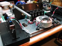
Thanks for that. I hadn't spotted that the T brackets are not exactly half way up the heatsinks!
Your caps look taller than mine, which is just as well because with the TeaBag PS they need to fit under the amp PCBs
I'm also using a white TeaBag PS, but yes the caps they are tall!

Also note that I drilled the heatsinks so they could be removed from the outside with the rest of the chassis intact.
BK
Attachments
I'm also using a white TeaBag PS, but yes the caps they are tall!
Also note that I drilled the heatsinks so they could be removed from the outside with the rest of the chassis intact.
BK
So organized! Just lovely.
I have (2) VFET builds that I am looking forward to...
Best,
Anand.
So organized! Just lovely.
I have (2) VFET builds that I am looking forward to...
Best,
Anand.
Anybody, have VFET kits or Vfet, that do not use or do not have time to do, please cede it to me
thanks
A quick question regarding R25,26,34,35 resistors which as per the build and BOM it says 221R 1/2W and I have some spare 221R rated @ 1/8W. The same with the R33 can I use 22K 1/2W instead of 22.1K?
Regarding the diodes can I use the "MUR160 DIODE, ULTRA-FAST, 1A, 600V" instead of the regular 1N4004?
Regarding the diodes can I use the "MUR160 DIODE, ULTRA-FAST, 1A, 600V" instead of the regular 1N4004?
A quick question regarding R25,26,34,35 resistors which as per the build and BOM it says 221R 1/2W and I have some spare 221R rated @ 1/8W. The same with the R33 can I use 22K 1/2W instead of 22.1K?
Regarding the diodes can I use the "MUR160 DIODE, ULTRA-FAST, 1A, 600V" instead of the regular 1N4004?
Ok I got the answers in the other thread.
thanks
1/8W is good enough for gate resistors
22K is practically 22K1
in this circuit , you can use MUR instead of 1N400x
Thanks Zen
Hi Folks,
I need some help and advice on my build because I'm pretty stuck right. I put together a DIY Audio Sony VFET kit a little while ago. I had no problems during the build with the testing as detailed in Nelson's article, both sides biased up well to ~ 100 mV across 32 with ~ 20 - 20 mV DC offset. To make a long story short when I powered it up the left channel worked just fine, the right channel sounded fine at very low volumes, but when the volume was turned up to normal levels the sound would fade out to silence.
So I double checked all of the components on the board and verified that they were all correct and the inboard readings on the resistors and test points agreed well between the two boards. A member suggested that
I test for AC across Pt 18 to gnd to see if the front end was working. I checked that and got mixed results so I assumed the JFETs were the problem and changed them out for new ones. On retest I got the same result, the right channel sounded OK at low volumes but the sound faded away when the volume was raised to normal volumes.
I suppressed the strong urge to smash things to smithereens with a sledge hammer and tripled checked everything on the board looking for possible shorts, cold joints, ect. All components were in the correct positions and I carefully reflowed every joint and cleaned the board of residue. I powered up the board to find that the offset on T18 - gnd had become 2.46v on the right board compared to the good board reading of 400 mV. So I'm thinking either there was a cold joint somewhere that affected the original adjustments, or a device on the board is faulty.
In the hope that a cold joint was the culprit I tried adjusting the pots to reduce T18-gnd while trying to get the bias across R32 but eventually backed the whole channel out of whack. So now my next step is to try and readjust the channel correctly with all of the components installed and the feed back loop operating. Can anyone give me pointers how to do this ?
One poster discussed grounding T18 then adjusting the bias on the back end. Would this be as simple as adjusting P1 to give me the correct voltage across T16 to gnd (12.7v in my case), and P2 to get the correct T17-gnd (-10.7v). Adjusting P3/P4 to get 1.2 v across R5 & R6 while minimizing T-18-gnd. Then shorting T18-gnd and biasing up the back end by adjusting P1/P2 to get 100 mV across R32 while minimizing DC offset ?
I would really appreciate any advise of direction on how to proceed.
Thanks,
Paul
I suppressed the strong urge to smash things to smithereens with a sledge hammer
I recall being in the same situation - you'll be surprise that grabbing some fresh air can give you fresh idea
I recall being in the same situation - you'll be surprise that grabbing some fresh air can give you fresh idea
We all have been there, and that is exactly what I did. I put the project aside for a few weeks to regroup for the next push. I'll post some pics when I get home tonite.
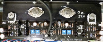
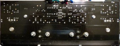
That was me that grounded T18 to setup the output stage independent of the FE. The FE offset at T18 needs to be low before attempting it (probably less than +/- 200mv). I only tried it because I had an unstable channel and Nelson had alluded to doing this somewhere in the main thread. My real issue turned out to be one end of the feedback resistor R3 not soldered. I think you should try to upload higher resolution photos if possible. I would also clean the back of the boards with isopropyl alcohol and scrub with an old toothbrush. Inspect with a magnify glass and make sure all solder beads/splashes are removed. I know you have probably done all this already but from the photos there still seems be a lot of solder splashes on the back of the board.
And with respect to the adjustment you are correct. This is exactly what I did :
One poster discussed grounding T18 then adjusting the bias on the back end. Would this be as simple as adjusting P1 to give me the correct voltage across T16 to gnd (12.7v in my case), and P2 to get the correct T17-gnd (-10.7v). Adjusting P3/P4 to get 1.2 v across R5 & R6 while minimizing T-18-gnd. Then shorting T18-gnd and biasing up the back end by adjusting P1/P2 to get 100 mV across R32 while minimizing DC offset ?
Except that the target voltage across R5/6 is actually 1.5v?
Last edited:
What's up with the frontend jfets? What types are they?
Also, don't just reheat solder joints. Remove the old solder and properly resolder with new, or add new solder when reflowing. Anything else is just asking for trouble. And remove residual flux as wineds already suggested. Some of the flux materials used are slightly conductive.
Edit: If all else fails, you may consider to (visually) take note of the current setting of the pots, turn them once fully clockwise and counterclockwise, and return them to their initial setting. This procedure may remove oxidation from the pots' wipers and ensure proper contact to the resistive element. Long shot, but still. It's also good practice to perform this procedure before putting a pot into a circuit.
Last edited:
Pass DIY Addict
Joined 2000
Paid Member
PJN: that bottom image of your board looks like it needs some careful inspection. It is hard to tell due to the smallish size of your image, but there are several rather tightly spaced solder joints there in the middle of your image that could be hiding some trouble for you. Take a flat-blade micro screwdriver and a bright light and physically scratch between ALL solder pads until you've lightly scored the circuit board itself. This will eliminate any inadvertent solder bridges. Sometimes they are so small that they are hard to see, but still form a solder bridge where one should not be.
I've posted this before, but perhaps this will help if I post it again here...
A few things that I do before ever applying power to any PCB I've stuffed:
1) measure EACH AND EVERY part BEFORE installing it on the PCB - I've been shipped 220k resistors in a bag marked 220R on multiple occasions
2) check, double-check, and re-check ALL installed components, orientation, placement, values vs the schematic, etc. Use the data sheet to understand which pin is which on devices that have more than 2 pins. Match this to the schematic and to the PCB before soldering. Solder all of the same devices (same jFets, same value resistors, etc) on both boards before moving on to the next part. Parallelism helps reduce errors.
3) if you are using brown Dale resistors, arrange legs so the resistor value points up and is readable when holding the board in your hand.
4) after soldering, take a fine flat-blade screwdriver and physically scratch between ALL solder pads on the back of the PCB (front, too, sometimes) to make sure there are NO errant solder bridges due to sloppy soldering
5) after mounting mosfets to the sink and BEFORE mounting them to the PCB, use your meter to measure each pin and make sure there isn't an inadvertent ground happening somewhere between the device and the sink. I've found problems in the past where a plastic collar was not seated properly, or when a tiny scrap of aluminum has pierced the sil-pad and grounded the device to the sink.
Hope this helps a little...
Last edited:
- Home
- Amplifiers
- Pass Labs
- Sony vFET Illustrated build guide