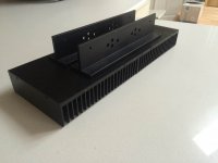
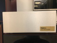
That is a nicely laid out amp
Thanks. The layout was driven by the size of the transformer. It is flatter and wider than the Antek/RKD equivalents. With that on the base plate, there was no space for the power supply boards - so, I mounted them on the front plates, which made assembly a pain! In the end, it worked out very well, as the 'flat' transformer was a nice distance from the signal boards and I could limit the power lines and the power supply components to the center of the chassis. The signal lines and power lines are nicely isolated. I have to say that it is a very nice transformer, though shipping to Asia was exorbitant......
Another front end bias question
Hi everybody,
I was able to build and bias front end and vfets on the 1st channel with no problems but the second channel seems harder to me. Resistor check was OK. Voltages good as well except for T6-T11 and T8-T13: +8.2V and -7.9V instead of ~5V. When I finally get to about 1.5V on R5 and R6 with as close to zeroV offset(T18-G) as possible, the DC offset doesn't seem that stable. After more than 30mn at 1.5V the DC offset runs up and down between about +120mV and -140mV. I can just sit and watch it go slowly back and forth over a span of about 15 minutes. Is that amount of fluctuation normal?
Another thing that seems funny to me, but I didn't really notice while biasing the first channel, is that the heatsink and the MOSFETs don't get warm at all. The only difference, build-wise between the two channels is that I used some keratherm pads instead the mica ones since I had cracked one of the mica ones. I checked and there's no continuity between MOSFETs and chassis. So don't think the insulator difference is a problem.
Also I should mention that at first I thought that fluctuation was caused by jfets, so, since I had an extra Diyaudio store matched B grade pair I switched them. Didn't make any difference.
Any help would be greatly appreciated.
Thanks
I also finished my amplifier recently. My voltages at T6-T11 and T8-T13 were also high at 7.3 to 7.5 volts at both channels. I don't think that is an issue as my amplifier plays music beautifully. I did run into what I thought was an issue with a large swing in cold versus hot offset measurements but I was told that it was normal. I asked about it in the Illustrated Build Guide thread.
The cold Mosfets do not seem right. The Mosfets in my amplifier definitely heat up. Are they cold in both channels? Have you hooked "test" speakers to the amplifier to see if it works?
I found that the front end and speaker offsets were greatly affected by temperature. I ended up placing the enclosure cover in place after each adjustment to try to maintain a stable temperature. Even after many hours I find that the front end and speaker offsets do fluctuate a bit over time, but not by hundreds of mV. I also found making small changes with some time in between for the temperature to stabilize worked best for the fine tuning. Also I concentrated on zeroing the speaker offset and allowing the front end offset to be higher. Apparently a front end offset of up to 200mV is acceptable.
If the Vfets are not warm, then there is not enough bias.
You can measure the current draw of the amplifier by taking the voltage
across the 0.1 ohm resistor.
Thank you Nelson (and BTW, thank you for making this all possible. I'm still a newbie but I've already built the Amp camp amps, an F5 and I have all the parts and boards ready to go for the Aleph J!)
I haven't installed the Vfets yet. I'm still at the front end biasing stage and was just wondering if the Mosfets were supposed to warm up at all.
However, even though I had already double checked that all the right parts were in the right places before posting my question, last night I decided to do that again with a higher powered magnifying glass and a small, very bright LED flashlight and lo and behold I spotted a tiny wisp of a solder bridge between two of the legs on Q3. I removed it and if I have time tonight I'll try again and report back.
Thanks again for all your help
- Home
- Amplifiers
- Pass Labs
- Sony VFET Amplifier Part 2


 i am very grateful for your kindness!!