Wow, I'm retarded
I really did look... sorry
For those of you like me who can't read, the multichannel AKM DAC used is the AKM AK4357.
I was suspecting this DAC while perusing the AKM website. It's the only one with DSD capability. Also, I'm suspecting the AK4383 is the other stereo DAC used on the additional separate stereo output (see Page 3-2 of DVP-NC650V Repari Manual). Again, this is the only 2 channel DAC that has DSD capability.
On a side note, I remember reading somewhere that AKM and Cirrus DACs were pretty similar. I find it intersting that the Cirrus 6ch. DAC (CS4362) with DSD capability has the exact same footprint as the AK4357....
Can anyone expand on the relationship between AKM and Cirrus? Are they partners? Sister companies? Thanks, just curious.
L8er (and I apologize once again for being retarded Dorkus)
power supply rails
ok i'm starting to get a feel for the different regulated rails we'll need for this project. from the block diagrams here's what i can surmise... C/S designates whether the rail should be constant (C) or switched w/soft power (S).
note the distinction between "C" and "S" is for my modified power scheme, not the original unit... the original power scheme is really messy and pretty nasty, e.g. the same +/-11V rails that feeds the analog stages also feeds the VFD and motors without a whole lot of filtering in between.  this new supply design should be much, much cleaner and give an appreciable improvement in sound quality. note that this will require moving the digital and analog board power connectors off the control board (CN407 and CN404), not a big deal. i've studied the block diagrams and schematics quite thoroughly and do not see any ill effect of these modifications on the functional operation of the unit - it should still work normally, with just the mains power switch removed altogether. more to come...
ok i'm starting to get a feel for the different regulated rails we'll need for this project. from the block diagrams here's what i can surmise... C/S designates whether the rail should be constant (C) or switched w/soft power (S).
Code:
    RAIL VOLTAGE    FUNCTION              C/S  NOTES
-----------------------------------------------------------------------------
1.  +/-11V          analog                C    also feeds +5V reg for DAC
2.  +3.3V           digital               S
3.  +5V             digital/control       S    also powers video output buf
4.  +11V            motor                 S
5.  +1.8V           digital supply        S    derived from 3.3V supply (2)
6.  -11V            VFD                   S
7. +3.3V control Cregulators
here are some suggested regulators for the different rails:
1. pass MOSFET w/zener reference (c.f. BOSOZ)
2. LT1763-3.3
3. LM1086-5.0 or equivalent
4. 7812 or equivalent
5. LT1763-1.8 (fed from #2)
6. 7912 or equivalent
7. LM1086-3.3 or equivalent
using 12V regulators for #4 and #6 should be ok, i do not foresee any problems. the actual voltage of the "11V" rails on the unit are more around 11.7V or so anyway. the problem with #3, #4, and #6 is that they do not have a shutdown feature - they're just standard 3-terminal chips. i'll keep looking for some inexpensive alternatives that feature shutdown, worst case we could use more of the (pricier) micropower regulators like the LT1763 which do have shutdown. i'm sure there are cheaper alternatives for this non-critical application though.
two split-bobbin transformers will be used, as they have better isolation than toroids which is important in a digital device. the analog should have something like 16V secondaries, digital can be a little lower since the IC regulators have lower dropout than the pass regulator. i'm wondering if feeding the lower-voltage digital supplies directly off the unregulated output will result in too much dropout across the device... in which case we will need to pre-regulate with a LT1085 or something. might not be a bad idea anyway, get some extra ripple rejection and regulation.
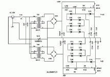
BOSOZ power supply
a.k.a. Balanzed Son of Zen...
schematic from Pass DIY document shown below.
obviously the transformer secondary, MOSFET gate voltages, etc. will be adjusted for this application. the resistors before the zeners on the gate will need to be reduced as well. bridge rectifier can be formed from HEXFRED or similar soft-recovery diodes. output of the regulator should be bypassed with something bigger, maybe 1000uF or so.
i've gotten good results with LM329 6.9V precision references, which have lower noise than generic zeners. each LM329 should be bypassed by a .1uF ceramic to resist oscillation (thanks Harry/Fred). i also use a small film cap in addition to the 10uF 'lytic to bypass the zener stack, but i don't know how good an idea this is. using two LM329's will yield 13.8V at the gate, but with a Vgs of 3 or 4 volts, the output voltage will probably be hanging around 10V... on the low side, i think 12V would probably be more ideal, but tolerable. if you absolutely must have +/-12V or greater, you can substitute different references that yield a higher value. be careful if you're using AD8260 tho, as it will only take +/-13V. for the 10V supply i suggest, a 32VCT transformer (16-0-16) should work ok.
Attachments
I just bought a Sony 500v and was wondering if the "Easy to
build I/V" posted by Lbhajdu in the Easy to build I/V thread
would be a suitable first mod for the 500v. I haven't opened my 500v yet and wonder how hard it is going to be to find where
to get the signal to bring out to an external I/V stage.
build I/V" posted by Lbhajdu in the Easy to build I/V thread
would be a suitable first mod for the 500v. I haven't opened my 500v yet and wonder how hard it is going to be to find where
to get the signal to bring out to an external I/V stage.
balanced outputs can be achieved very easily in this unit by changing the output stage from a single opamp in differential-input configuration to two single-ended stages (buffer, opamp, whatever). not sure what player Pam has modified but it is easy to do with the AKM DAC-based units, as well as the higher-end ES players which use dual-differential DAC configurations or have inherently balanced DACs.
hi jam,
oh yeah. trannies are nice. has a LPF effect as a nice side benefit as well. i may actually consider using a xformer to sum the diff outputs of the DAC, then use a simple JFET buffer after that. maybe Jensen xformers? not sure how the DAC would respond to that type of inductance though.
oh yeah. trannies are nice. has a LPF effect as a nice side benefit as well. i may actually consider using a xformer to sum the diff outputs of the DAC, then use a simple JFET buffer after that. maybe Jensen xformers? not sure how the DAC would respond to that type of inductance though.
Marc,
The Jeff Rowland web site has some good articles on the use of transformers.
http://www.jeffrowland.com/techtalk.htm
Jam
P.S. How goes Son Of Dork?
The Jeff Rowland web site has some good articles on the use of transformers.
http://www.jeffrowland.com/techtalk.htm
Jam
P.S. How goes Son Of Dork?
clock circuit
while i've had my mind on power supply and analog stage possibilities lately (which are related of course), another member of this project, Blair, has been diligently working on the clock circuit. Blair is an engineer at a specialty oscillator firm so he knows his stuff:
Blair is also going to try to get some jitter measurements out of the NS500V if he can. thanks for the great info!
while i've had my mind on power supply and analog stage possibilities lately (which are related of course), another member of this project, Blair, has been diligently working on the clock circuit. Blair is an engineer at a specialty oscillator firm so he knows his stuff:
I have had a bit more of a think about the clock circuit and I think it would be best if we went with a CMOS output oscillator connected to the XT IN pin and tie XT OUT to ground through a resistor in series with a capacitor, we may have to leave XT OUT open depending on the internal ocillator configuration of the pll.
The advantages of the CMOS OSCILLATOR ARE AS FOLLOWS.
1: High slew rate 2 ns reduces potential edge jitter problems.
2: High signal level with low output impedance good drive capability high noise immunity.
Unfortuately the CMOS oscillators we design at work are unbalanced supply rail referenced ( not differential ) this means they would be affected by ps noise still but if we cleaned up the ps rail then this would not be such a problem.
This type of oscillator at 27 MHz would have approx 6 ps jitter over a bandwidth of 1Hz to 100 KHz before going into the pll.
I don't really know if the pll is that noisy if sony have managed to acheive a measured jitter spec of 190 ps. Other players jitter measurement have not been much better and they don't use a pll to generate the other clock frequencies needed.
The PS rail to the pll should be as clean as possible otherwise you would loose a lot of the advantages of feeding it with a low noise oscillator. The cmos output of the pll is probably supply rail referenced as well so ps noise will cause jitter.
If we go for seperate clocks there could be a problem with clock synchronization as the MCLK should be synchronized with the DSD clock ( DCLK ) for the AK4383 2 channel DAC.
Blair is also going to try to get some jitter measurements out of the NS500V if he can. thanks for the great info!
Anyone still have the service manual for the 500v?
I am looking to resurrect my long dead 500V (it went belly up years ago, only the red light comes on when I turn the power on). My skills and knowledge have improved since then, and I would like to work on the 500v and see what I can do with it.
It would be helpful to have the service manual, and I'm wondering if anyone who happens to read this still has the service manual and would be willing to share. I'd love to have the manual for the AKM4357 and AKM4383 I would appreciate it.
Thank you for your time and consideration.
Best,
Aaron.
re: long dead 500V ???
when I power mine up, the lcd display momentarily says the word standy, the power led blinks green then it goes red again. pushing a button like tray open will turn the unit on and change pwr led to green. does your unit do the same thing or just a solid red led without a momentary blink to green? also, a long time ago, i thought i downloaded a copy of the akm data sheets in pdf. i will let u know if i can find them.
Dorkus may have also posted some partial schematics on the "My hacked up ns500v" thread a while back, AFAIK
I am looking to resurrect my long dead 500V (it went belly up years ago, only the red light comes on when I turn the power on). My skills and knowledge have improved since then, and I would like to work on the 500v and see what I can do with it.
It would be helpful to have the service manual, and I'm wondering if anyone who happens to read this still has the service manual and would be willing to share. I'd love to have the manual for the AKM4357 and AKM4383 I would appreciate it.
Thank you for your time and consideration.
Best,
Aaron.
when I power mine up, the lcd display momentarily says the word standy, the power led blinks green then it goes red again. pushing a button like tray open will turn the unit on and change pwr led to green. does your unit do the same thing or just a solid red led without a momentary blink to green? also, a long time ago, i thought i downloaded a copy of the akm data sheets in pdf. i will let u know if i can find them.
Dorkus may have also posted some partial schematics on the "My hacked up ns500v" thread a while back, AFAIK
- Status
- This old topic is closed. If you want to reopen this topic, contact a moderator using the "Report Post" button.
- Home
- Source & Line
- Digital Source
- Sony NS500V SACD modification project