terry:
just had a very quick look at the schematic.
two things hit me right away:
1. i wouldn't build this unless i wanted to smoke the cascodes Q3 & Q4; they are not biased properly
2. if D6 is really an LED, (lets say it's red) is 1V across Q11 and Q12 really enough for them to operate properly? i'd guess not ...
there's more, such as <1ma seems small amount of bias for LED D6 to be used as a voltage reference ...
mlloyd1
OK, as I said I am trying to learn. All of the values are per the original schematic. I probably need to adjust some things for the lower voltage. This IPS was designed to run between 55v & 70V. R16 probably needs to be lowered to get the amps right on D6 (blue). Q3&4 are running at 1.3mA. Is that too high?
EDIT: You got me curious because I hadn't played the Symasui IPS on lower voltages so I just went out and hooked it up to my baby Slewmaster. It plays perfectly fine at +-40V rails. Not sure why is looks bad on the sim.
Last edited:
terry:
just had a very quick look at the schematic.
two things hit me right away:
1. i wouldn't build this unless i wanted to smoke the cascodes Q3 & Q4; they are not biased properly
2. if D6 is really an LED, (lets say it's red) is 1V across Q11 and Q12 really enough for them to operate properly? i'd guess not ...
there's more, such as <1ma seems small amount of bias for LED D6 to be used as a voltage reference ...
mlloyd1
Hi Mlloyd1,
In fact, those are fine.
1. Actually the cascode is just tied to -12V, formed by Zener, so it is fine. No smoke
")
2. D6 id LED, I believe a green one... Q11, Q12 work at low Vcb, but enough for normal operation. I tried configuration with even lower Vcb - worked perfectly (see attached example, Q1 works at extremely low Vcb).
So no worries.
Cheers,
Valery
sorry, false alarm on Q3, Q4 - i didn't see R13 down there.
at first, i didn't think there was a proper voltage divider at the cascodes bases and the 22ohm base stopper went straight to -VCC.
never mind, they'll live
mlloyd1
Yeah, it's just drawn in a bit confusing way...
OK I just checked again and bringing the amp up on a variac, the blue LED (D5), comes on almost instantly but the red LED, (D5) doesn't come on until about +-36V. Should R11 and R13 be lowered for using the lower voltages?
Also, getting back to the little MOSFET OPS, I had a typo earlier. Q13 and Q14 in Jason's schematic above are running at 15mA. Do they need a heatsink?
Any other suggestions about the small OPS?
Thanks, Terry
Also, getting back to the little MOSFET OPS, I had a typo earlier. Q13 and Q14 in Jason's schematic above are running at 15mA. Do they need a heatsink?
Any other suggestions about the small OPS?
Thanks, Terry
I found at lower voltages R13 needed to be a lower value to get the Zener on the negative rail to bias properly. I would put Q13-Q14 on a small common heat sink with the VBE multiplier. We could use a non thermally connected diode in the VBE emitter circuit like we did with the vertical MOSFET modification to tailor thermal compensation if the plain VBE arrangement overcompensates.
We want some current in the EF stage, that is what drives the MOSFET gate capacitance. The price paid is some dissipation in those driver devices. That said the 47R may need tweaked in the real implementation, so yes, we can alter the value if need be. I'd target 12-16mA in the EF stage and 120mA bias in the outputs. Those numbers seemed to work well with the VSSA and I suspect they will work here too.
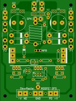
A stripped down bare bones lateral MOSFET OPS the same size as an IPS (3"x4") might look something like this:
But, I think it better using 3 mosfet, then we mount 1, 2, or 3.
The bias servo could optimize to both vertical and lateral. May be LED can be changed by jumper for lateral.
Experiment in progress, enter at you own risk!
OK, gents. This is a 'use at your own risk', 'no warranty, expressed or implied' type deal. I'm pretty sure this is free of errors (did a little quick clean up) but since I haven't made one to test I can't say that it 'just works'. Enjoy.
Oh, and if it does work, post some pics!
OK, gents. This is a 'use at your own risk', 'no warranty, expressed or implied' type deal. I'm pretty sure this is free of errors (did a little quick clean up) but since I haven't made one to test I can't say that it 'just works'. Enjoy.
Oh, and if it does work, post some pics!
Attachments
But, I think it better using 3 mosfet, then we mount 1, 2, or 3.
The bias servo could optimize to both vertical and lateral. May be LED can be changed by jumper for lateral.
Bimo, yes for a truly practical implementation I would agree. This is born out of an idea / desire Terry had to 'just give it a try'.
The LED will give some uncompensated spread for the lateral MOSFETs and the rest of the VBE multiplier will compensate the drivers. I haven't worked out the values to use in the lower resistive leg of the VBE to get the spread we are after and sim won't help much because the threshold voltages of the laterals isn't realistic. Just FYI, it might take some trial and error.
Last edited:
Output PCB layout question...
The most common output PCB layout mounts all of the NPNs on one side(edge), and all of the NPNs on the opposite side(edge). Bob Cordell has commented that inductance*current*resistance_gradient noise from the output currents can be reduced by interleaving one NPN next to one PNP evenly along both sides(edges) of the PCB, such that the output noise is significantly cancelled by the adjacent opposite currents in the layout traces.
Has anyone experimented with alternate NPN_PNP_NPN_PNP output PCB layouts?
- Home
- Amplifiers
- Solid State
- Slewmaster - CFA vs. VFA "Rumble"