Both are MUR160, but anyway please note the post number where you saw this difference.")
Thanks, I must seach in the post as a save schematics on my PC.
Marc
Lasy Cat i look and found several schematic.
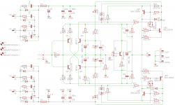
#post 217 and 401 where there is 2x mur 460 and un 1k resitor between mosfet driver Gate and Collector from more "inside" BJT in BiGBT
#post 434 (it'this schematic i use) there is one mur160, one mur460 but the 2x1k disappear.
Marc
#post 217 and 401 where there is 2x mur 460 and un 1k resitor between mosfet driver Gate and Collector from more "inside" BJT in BiGBT
#post 434 (it'this schematic i use) there is one mur160, one mur460 but the 2x1k disappear.
Marc

#post 434 (it'this schematic i use) there is one mur160, one mur460 but the 2x1k disappear.
Marc
Marc, I understand that you are a little confused, but the function of the MUR160/460 diodes is only to prevent reverse polarity between emitter and collector of the output transistors because of the EMF causing reverse inductive potential from the speaker's drivers. The diode forward current of 1A from MUR160 is completely enought to withstand at 0,7V, not allowing the reverse voltage to rise over that limit. In my design of BIGBT I used MUR460 also because other important reasons, not only the current capability. So once more, you can use MUR160 without any worries.
Two 1k gate-source resistors didn't disappear, they just change location outside BIGBT box, cause this is no longer metal case module like I have here by me, it is BIGBT located on Alex's PCB.
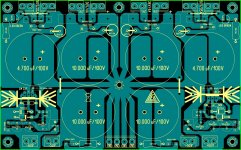
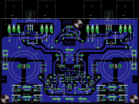
So i redrawn and adapt to my own requierement Alexmm pcb fromm basic SSA_BIGBT (35V rail).
Double rectifier bridge,2SA970/2SC2240 intake, MJL3281/MJL1302 output.
See attached files
Nice board.
I am currently working on a customized schematic in Multisim.
It works great with low distortion and no instability (in the simulator), but the DC offset and bias is kind of funky. I'm not understanding.
But, hopefully I will figure it out and put it on a PCB and test it. I have alex mm pcbs to look at for help now.It is an SSA running off of +-50V rails (both input and output stage), using two pairs of NJW1302/3281 in an EF output stage. I'm not experienced designing anything so I am expecting to learn from problems with this.
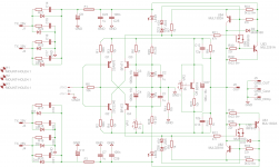
Hi Idefixes!So i redrawn and adapt to my own requierement Alexmm pcb fromm basic SSA_BIGBT (35V rail).
Double rectifier bridge,2SA970/2SC2240 intake, MJL3281/MJL1302 output.
See attached files
Nice PCB !!
Is this the final PCB and tested, because we want making this amplifier at this PCB?
Or to wait a bit?
Thanks and cheers!
Hi Idefixes!
Nice PCB !!
Is this the final PCB and tested, because we want making this amplifier at this PCB?
Or to wait a bit?
Thanks and cheers!
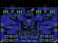
Not testeing for moment, i need to recheck it and etch it. Are you shure you can have matched Hfe output NPN//PNP...it's needed for BIGTB configuration. Often NPN and PNP batch have quite different Hfe range. Exemple : my 100u 1302 were between 75 and 85 hfe and my 100 3281 were between 80 and 140 with only a few matched..
So i redrawn and adapt to my own requierement Alexmm pcb fromm basic SSA_BIGBT (35V rail).
Double rectifier bridge,2SA970/2SC2240 intake, MJL3281/MJL1302 output.
See attached files
Very nice PCB, it will work, no doubt about that. The only issue I see are the fuses. On this position they secure complete board except rectifiers so in that point of view it would be better to put them at each AC input from the transformer secondary. Also their value must be a lot higher than really needed for protection because of initial C9 & C11 charging current. Now they're not protecting output transistors from overcurrent faulty condition, because C9 & C11 will provide deadly current peak to outputs anyway. So if you would like to successfully protect the output BJT's you'll have to connect the fuses after big caps.
Not testeing for moment, i need to recheck it and etch it. Are you shure you can have matched Hfe output NPN//PNP...it's needed for BIGTB configuration. Often NPN and PNP batch have quite different Hfe range. Exemple : my 100u 1302 were between 75 and 85 hfe and my 100 3281 were between 80 and 140 with only a few matched..
Hi
What are the resistors R15 and R19 of 5W?!
Thanks
Hi Mr.Yes 5W. I will put 10 0.6w 1% 2.2r in //
Marc
So when will it be smuggling commerce?!
What do you recommend you output transistors!
The match took 1978year 2N3055, Mr. now the 21-century!
As long-matching ... please !!???
thanks
P.S.
Where is the RCA???!
Where are you French?!!!
Cheers
Last edited:
Hi Guys, sorry I have been on a business trip for the past week and do not carry a notebook with me. The progress I see is exceptional.
If I may I would like to point out something that may affect your view of fuses. Fuses have two functions and these may not be related. Fuses are normally used to prevent fires, through prolonged fault conditions. In that case placing the fuse in the AC path as LC recommends is valid. This means the fuse will blow in the event of devices going faulty and the board/wiring starts to burn. A fuse should always be used when changing from a large wire dimension to a smaller wire dimension.
Fusing of the incoming mains to the transformer is normally sufficient and if it blows you do not have a possibility that a faulty component swings the output to one rail and remains there.
The configuration I used it in the MOSFET version (besides fusing incoming mains) is really for protecting the speaker and not dump the capacitor's stored energy into a speaker should a fault occur since I never use speaker protection, this has worked well for me.
Anyway this last comment is open for debate, it is not a hard and fast rule, but that you need to protect against fire hazard is essential.
Kind regards
Nico
Very nice PCB, it will work, no doubt about that. The only issue I see are the fuses. On this position they secure complete board except rectifiers so in that point of view it would be better to put them at each AC input from the transformer secondary. Also their value must be a lot higher than really needed for protection because of initial C9 & C11 charging current. Now they're not protecting output transistors from overcurrent faulty condition, because C9 & C11 will provide deadly current peak to outputs anyway. So if you would like to successfully protect the output BJT's you'll have to connect the fuses after big caps.
Lasy Cat i modify the pcb based on your advice.
Marc
Attachments
Hi Mr.
So when will it be smuggling commerce?!
What do you recommend you output transistors!
The match took 1978year 2N3055, Mr. now the 21-century!
As long-matching ... please !!???
thanks
P.S.
Where is the RCA???!
Where are you French?!!!
Cheers
My english is not on top so i have some difficult to understand you. You can take the output BJT you want as you match PNP and NPN on HFE in each BiGBT module. The pcb is based on Alexmm, the signal intake point located the same. Between the two 1000u/16V caps. For me it's a 2.5mm molex connector.
Yes i am French.
Marc
- Status
- This old topic is closed. If you want to reopen this topic, contact a moderator using the "Report Post" button.
- Home
- Amplifiers
- Solid State
- Simple Symetrical Amplifier