Dear CBS240,
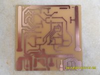
I will implement the suggested changes in a simulation cenario and see how it works. I believe I have room on the PCB for the changes. I am posting the PCB picture (copper side) so you can have a look at it.
I will keep posting the results as I make the changes.
Regards,
Elton.
I will implement the suggested changes in a simulation cenario and see how it works. I believe I have room on the PCB for the changes. I am posting the PCB picture (copper side) so you can have a look at it.
I will keep posting the results as I make the changes.
Regards,
Elton.
Attachments
Still, I would only add cascodes to the input LTP and maybe omit caps to be complete DC coupled. That would be almost perfect for this kind of design.")
Cascode of the input stage is not a bad idea, but the purpose of the cascode I added in the VAS is not so much for the conventional benefits of a cascode but to allow the same Vce bias voltage across the VAS differential transistors so that they will exhibit the same Pd with the equal current, as such they should be bias with. I would not omit the input and DC blocking caps for this design. This is a learning experience and should be constructed and understood in steps. The omission of the DC blocking cap would be accompanied by a DC servo circuit that would replace the function there of. True it would be better but......
One step at a time.
I suggest following through with the already produced PCB and then determining the faults in layout ect. You can always transfer the used components to another improved PCB later. Trust me, I do this all the time. If I spend $8 a piece for THAT matched transistor arrays in an experimental project, I am going to use them again in something else.
 You have already made the PCB, modify the PCB if necessary to make the circuit work, then produce a new and improved PCB. Step by step.
One thing to keep in mind is that PCB copper has resistance, be it very small, but to many ampers of current it is significant. There should be the same amount of copper size and distance from the source pins and balast resistors to the output. IOW, the physical distance between each source and the output terminal should be equal. Doug Self explains this in some of his research.
New project
Dear all,
dorynetz1, the amplifier is working fine with +60v and -60V with only one pair of IRFP.
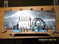
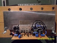
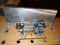
I am now working in a new project. A High Power Amplifier. The board is already ready and I am now running the tests. At the moment I have managed to get 68.3 V on the output with a 4 ohm load.
I will post some pictures after finishing the tests.
Regards,
Elton.
Dear all,
dorynetz1, the amplifier is working fine with +60v and -60V with only one pair of IRFP.
I am now working in a new project. A High Power Amplifier. The board is already ready and I am now running the tests. At the moment I have managed to get 68.3 V on the output with a 4 ohm load.
I will post some pictures after finishing the tests.
Regards,
Elton.
High power amplifier
Dear Andrew,
I only have a 4 ohm load at the moment. 68.3 VAC measured at 1KHZ. It is an AB class amplifier. The power supply is very robust. It uses a 2600 VA toroid transformer, 2x35A rectifier bridges and 3x6800uF capacitors per line (3 capacitors for + and 3 capacitors for -).
I will get another 4 ohm load to test it with 8 ohm load. I will let you all know the results after the tests.
Doing simple maths, in 4 ohm load, we would have something around 1100W. My speaker is a 15" 4 ohm 1100W RMS by Selenium. Selenium is a Brazilian company that is now together with JBL.
As it is I have to be very careful not to increase the output power so much if I do not want to burn my speakers. I have not tested the full power on the speakers yet since I have not finished the construction of the cabinets. I will be using 2 JBL 4530.
Regards,
Elton.
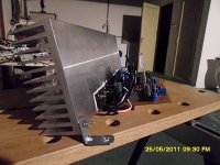
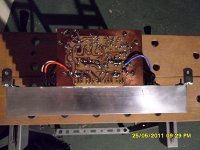
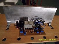
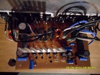
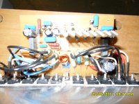
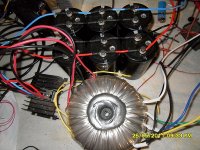
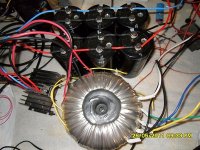
Some pictures.....
I am posting some pictures of the board an power supply.
I am posting some pictures of the board an power supply.
Attachments
-
 SDC10001a.jpg179.2 KB · Views: 173
 -
 SDC10002a.jpg177.1 KB · Views: 153
 -
 SDC10003a.jpg177.5 KB · Views: 154
 -
 SDC10006a.jpg178 KB · Views: 53
 -
 SDC10005a.jpg177.8 KB · Views: 55
 -
 SDC10004a.jpg176.4 KB · Views: 141
 -
 SDC10007a.jpg178.8 KB · Views: 49
 -
 SDC10008a.jpg185.3 KB · Views: 70
 -
 SDC10009a.jpg200.6 KB · Views: 59
 -
 SDC10010a.jpg201.9 KB · Views: 63
If I make a new design I put a DMM across one of the source resistors and watch the voltage. I let the amp warm up with music and monitor the voltage.
Another simple trick with a Vbe multiplier is putting a zener across it to stop too high a voltage destroying the output transistors.
I have a testbed for amplifiers that uses a low current transformer for testing amps.
If I get a short then the output mosfets dont blow as it is only a 2 amp transformer.
So long as I dont let things cook too long the transformer is fine.
Last edited:
- Status
- This old topic is closed. If you want to reopen this topic, contact a moderator using the "Report Post" button.
- Home
- Amplifiers
- Solid State
- Simple mosfet amplifier