zigzagflux said:
What about the possibility of the attached current source?
No difference.
Good work, wrenchone!
mach1 said:wrenchone,
if you can find any cheap 6AW8, the triode section is a real sleeper: u=70 Rp =17,500 and sounds excellent.
pm
Shhhhhh! Ixnay on the 6aw8 alk-tay. You'll knock up the ice-pray. Note how I cleverly camouflaged the topic by mis-labeling it a 6aw6.
")
http://www.diyaudio.com/forums/showthread.php?s=&threadid=88001&perpage=10&highlight=&pagenumber=1
I took another look at your schematic and noticed that you were closing the loop around the output tube rather than the input. Can you expound?
The input tube makes very little distortion, and the distortion that it makes is almost all 2H which is musically rather benign. If that stage makes no offending distortion, why mess it up with feedback.
All of the above sounds like good theory, and I believe in using only as much feedback as necessary, only where it is needed. I tried various feedback combinations when designing the amp, and settled on cathode feedback for this design because it seemed to do the job. I use a feedback switch that allows the feedback to be disabled if desired. The amp shown in the picture is hard wired for zero feedback. (variable feedback control under development)
Cathode feedback can do wonders to clean up the sound of a cheap OPT. The results are highly dependent on the transformer itself. The Hammond 125 series, and any Edcor that I have tested benefit greatly from cathode feedback, while some other transformers don't benefit as much (good ones). It seems to work well in UL mode amps with most transformers (lowers output Z). With some transformers (Edcors) 3 to 5 db of feedback can cut the measured distortion in half. The sound is obviously cleaner and the bass is tighter. The same amount of feedback applied globally doesn't yield the same sonic or measured benefits. I have also found that you can (in some cases) apply more cathode feedback than you can get away with globally before the sound goes limp.
I did a comparison test between the big Edcor OPT and the Hammond 1628SEA. At the end of each test there is a graph where the distortion VS power is plotted with and without CFB in UL mode. For either transformer the distortion is almost cut in half with 5 db of CFB. If you study the last graph (Edcor in UL), look at a given distortion level, say 5%. Applying cathode feedback effectively DOUBLES the amplifiers output power. It is almost like wiring in a second tube! Granted the big Edcor transformers are a unique case, they have a lot of built in distortion in UL mode, but it cleans up nicely. These transformers sound far better than they test, especially if you want to get loud. They make more power than the Hammonds (so do their little ones), and they just sound louder than the Hammonds at the same power level.
http://www.tubelab.com/Output_Transformers.htm
I dropped in the JFETs and 6C4 cascode tubes last night (after rewiring the sockets). It looks as though I should be able to ditch the current source loading and go back to a resistive load (say 33k) and still have gain to burn. The lower JFET will set the stage bias current at 5ma with the source resistors I've selected.
zigzagflux said:Interesting analysis, and easy to overlook these stray capacitances.
What about the possibility of the attached current source? I have even considered replacing the LED with a few series schottky's, which have extremely low capacitance and excellent high frequency behavior.
It would appear to me that the capacitance path you have identified would be mitigated/minimized, yet still keeping the same basic design. I would even think you could reduce the 1uF cap by a factor of 10 and not really affect the performance all that much. LM285 has very low dynamic impedance.
Zigzagflux,
Sorry for my late reply, but I just now saw your post and question. The capacitances that I refer to are intrinsic to the physics of solid-state devices. I do not tend to think of them as "stray". Maybe it’s just semantics, but to me "stray" implies external capacitances between two conductors and is very much layout dependent. While we generally want to keep those low too, strays are usually not signal dependent (non-linear), but they may be microphonic, a topic for another day.
I do not think that your circuit solves the Ccb loading problem, unfortunately. The plate resistance "sees" the Ccb of the MJE350 as if it were grounded directly at the base end, because the base end of Ccb is AC grounded through the LED (or even through your Schottky replacement), through the 1uF, and then through the PS capacitance to ground. Whatever series impedances these parts offer at high frequencies is trifling compared to Ccb, and they may be considered shorts to ground in most cases. As someone mentioned earlier, it’s hard to solve this problem by adding an isolating resistor to the base of a BJT like the MJE350, because it will drag down the performance of the BJT. A MOSFET, which may have an even larger Cdg, can at least profit from a large-value resistive divider to set the DC gate voltage, but even that provides a feedback path from drain to gate, possibly modifying behavior at high frequencies. As I’ve recommended before, I would refer you to Gary Pimm’s CCS work, not as the only possible solutions, but as a good reference on how to eliminate the shunt C, at least to a very large extent.
mach1 said:Is the capacitance change under dynamic conditions always proportional to the measured static shunt capacitance, or is it possible that some CCS' with a fairly high Cs display very little dynamic change?
I am very interested phase intermodulation effect and the psycho-acoustic implications. Could you point me in the direction of any papers that have been published on the subject ?
regards
pm
Mach 1,
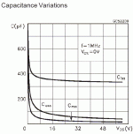
Sorry for my late reply, but I saw your post and question only today. You ask a very good question. As a first order consideration at least, my thought is to make the absolute value of the “visibility” of the semiconductor device’s interelectrode capacitances as low as possible, with the assumption that the percentage variation ought to be lower too. However, if you look the problem in more detail, you will see that these C variations are not necessarily constant percentages of their absolute Cs. Variability depends a lot on the currents and voltages they see. There are three interelectrode capacitances for each three-legged semiconductor, with different physics for BJTs, MOSFETs and JFETs. So it’s hard to generalize, but in all cases there are non-linearities. For our purposes in designing CCSs, we usually would concern ourselves with collector or drain capacitances. The attached picture, as an example, shows the behavior of the capacitances in the IRF820 MOSFET. The MJE350 data sheet is not enlightening about capacitance, but all BJTs show non-linearity in the capacitance of the reverse biased collector-base diode. For the MOSFET, note that percentage change of the capacitance tends to be worse at low voltage values; so a design implication is to bias with higher voltages. But there still is a slope (variability) even at high voltages. My belief, unproven, is that even very tiny amounts of this variation can be audible.
There is precious little written about this topic as it relates to audio. I think phase intermodulation explains to a great extent why tube and transistor audio circuits sound different. I have been gathering research material and doing my own tests, but I’m not ready to promise an article yet. I draw a lot from digital audio work, where it has been discovered that extremely tiny values of jitter can be audible (in the range of hundreds of picoseconds, if not even lower). Since capacitance variation may be thought of as time-domain signal-dependent jitter, or as phase intermodulation distortion, there is relevance between analog and digital. Malcolm Hawksford has drawn the parallel in one or two of his excellent papers. Bob Cordell wrote on the subject of phase intermodulation (I notice that he posts in DIYAudio from time to time). He also proposed a test instrument for measuring phase intermodulation, separating it from the more typical amplitude intermodulation that we think of with regard to IMD. Papers about the audibility of digital jitter have been written by Dunn, Hawksford, Meitner, Willenswaard, Manson among others (refer to the AES and IEEE archives).
Attachments
Attached is the latest incarnation of the "Shrine" amp. I've ditched the current source loading and am using a JFET input cascoded with a triode. I'm going to fire up the circuit sans feedback to check the overall gain, and if it's what I expect, I'll be applying some feedback to the JFET source. Next in line is buring in the SMPS. Unfortunately, events (like a computer trash) have kept me from giving this project the attention it deserves. Hopefully, I'll be able to box it up soon, and give it a place of honor in the living room...
Attachments
I'll be driving the amp from a solid state source, so 47k is just fine. Even if I were to use a vacuum tube preamp, I would design one with a cathode follower output. In general, I don't like using really high impedance terminations on inputs available to the outside world.
Next pass - I let my SMPS warm up on the bench today with resistive loading, and it settled in at around 85.3% efficiency at 115VAC input, using a sine wave source. The efficiency calculation assumes that the load resistors are dead on at 3.6k and 9 ohm load for the 350V and 12.6V outputs, respectively. Since the resistors are 10% tolerance, the efficiency could be a little off either way - I was too lazy to break the output connections and insert ammeters. Nothing is getting hot, so the losses are pretty evenly spread out.
Conducted EMI needs a little work, but I'm pretty sure how to fix it. As I expected, the really high frequency noise is down in the mud using a self-oscillating supply. I expect another rev on the transformer will help tame down the EMI. I may also look at a better layout that I've done since this one, as I suspect the primary swiitching FET may be a little too close to the input common mode choke in the original incarnation of the supply. I may also try grounding the FET heat sink to primary return through a resistor. I'm using a full-pack TO-220 FET, so that the drain is not directly nailed to the heat sink, but the sink may still be acting like enough of an antenna to mess up the conducted EMI.
Conducted EMI needs a little work, but I'm pretty sure how to fix it. As I expected, the really high frequency noise is down in the mud using a self-oscillating supply. I expect another rev on the transformer will help tame down the EMI. I may also look at a better layout that I've done since this one, as I suspect the primary swiitching FET may be a little too close to the input common mode choke in the original incarnation of the supply. I may also try grounding the FET heat sink to primary return through a resistor. I'm using a full-pack TO-220 FET, so that the drain is not directly nailed to the heat sink, but the sink may still be acting like enough of an antenna to mess up the conducted EMI.
Ok - this thread rises from the dead. I've done a lot of fiddling off and on over the months with my SMPS to minimize EMI - not the simplest proposition, as both the primary and HV secondaries are a source of RF racket. Transformer design is crucial, as well as grounding the primary switch heat sink and the transformer core to primary HV return.
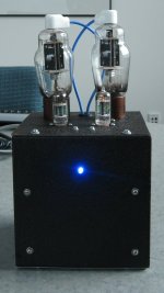
The amp and power supply were integrated last Saturday for a showing at the Burning Amp fest in San Francisco, and I got everything buttoned up and working satisfactorily. I didn't get a chance to audition the amp at BA, which was a shame, as there were a number of high efficiency speakers there that would have been a nice match. People did ooh and aah over the small form factor, though. So far, I've been confined to using the Paradigm Monitor 7s we use at work for audio testing (they call 'em Paradigms 'cause I wouldn't give a pair o' dimes for them...). Not the most efficient speakers in the world, but the amp will drive them to reasonable levels. The major bottleneck is the tiny Edcor output transformers I used. I can easily get the transformers to saturate with difficult material at high volume. This amp is definite inducement to complete the ported MTMs I have in the works.
Pictures, updated schematics, and some performance stuff will follow when I have a little more time for documentation. This is the first in a suite of compact amps using SMPS.
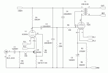
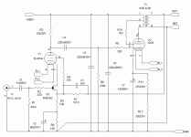
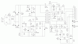
This is the final schematic for one side. Inside the amp, the two 1625 filaments are connected in parallel, and the 6C4 filaments are in series. The filament voltage on the SMPS is tweaked up by about a volt, and a 5 ohm inrush limiter is connected in series with the filament supply. This keeps the cold filaments from going ballistic when confronted by the SMPS at turn-on. The thermistor gracefully warms up and leaves the filament supply at ~12.7V.
This is really the schematic I intended to attach to the last post. Comments from the last post still apply. There really isn't anything too much out of the ordinary about the circuit except for the JFET in the first stage. This is something I've seen used in classy RIAA preamps, but not in a power amp. I did it for the gain, so I would have something to feed back to lower the output impedance.
Attachments
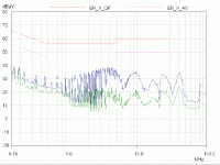
Here is an EMI scan of the complete amplifier, with no cables connected except for the power cord. Things are pretty good until you get to the high frequency region. The big bump and assorted rubbish beyond 30MHZ are a bit of a mystery, since self-oscillating flybacks are suposed to be pretty quiet in the very high frequency region (comments, Eva?). It may be because I'm using a discrete bipolar SCR to turn off the primary switching FET (fast). It may also be that the 1625s are singing soprano, something they and their 807 brothers are prone to doing. I'm trying some plate snubbers in the classical manner tomorrow to see if this helps. My ultimate solution (if the 1625s are not at fault) is to replace the current self-oscillating flyback supply with a ZVS (zero voltage switching) flyback supply, which should be a lot quieter and more efficient to boot.
Attachments
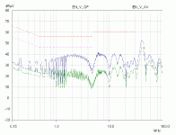
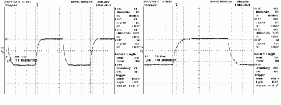
An explanation of the previous EMI scan - the limit lines shown are the EN55022 limits both average and quasi-peak measurements, and the traces shown are the average (lower trace and limit) and quasi-peak (upper trace and limit). A pass with 6 dB of margin is OK, and a 10dB pass is quite good. Most of the EMI spectrum has 15dB margin. The disturbing stuff is the > 30 MHz rubbish. More on that later. Attached is the amplifier 10kHz square wave response into a 10 ohm load (closest power resistor at hand). I think I can get a little faster response and still slightly overdamped by using 2.2 nF of compensation instead of 3. (when I was working on the loop a couple of weeks ago, I only had increments of 1.5 nF at hand, and one was not quite enough).
Attachments
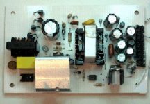
Attached is a schematic for the power supply. There is no SMPS controller chip. The design type is generally referred to as a "ringing choke converter" or "self oscillating flyback", and if you load Google with those search terms, you'll be rewarded with some basic background info and papers. I chose this design because it runs in borderline discontinuous mode, making it appropriate for high voltage outputs. I also chose it because the pirmary FET switches fairly slowly and generates less EMI (in theory). I learned quite a lot adapting this sort of design for powering vacuum tubes. The dV/dt on the HV outputs makes EMI more of a problem than a design with low voltage outputs.
One particular problem with multiple output SMPS is output sequencing. I used the DC filament outputs for feedback to set output voltages, especially as I wanted the filament voltage to be tightly regulated. A thermistor connected in series with the filaments (not shown) limits inrush current. When the supply is first turned on, the filaments are cold, so the plates draw no current, and the HV output shoots up to 470V from a nominal value of 350V - not nice, both for the tubes and the output filter caps. The Neanderthal way of solving the problem would be to use a substantial preload resistor on the HV output. I instead used a series zener string (380V total) connected to the summing node of the filament voltage sensing divider. When the HV overshoots, the zener chain conducts and limitts both the HV and filament voltage excursions until the filaments warm up and the tubes start drawing current. This has an added benefit in that it provides additional soft start for the tube filaments.
I added snubbers to the output rectifiers and some additional EMI filtering inside the amplifier chassis, which definitely did some good.
Attachments
This is the EMI scan with the power supply modifications. The HF end has improved. This will do until I can construct a quieter power supply using a zero voltage switching flyback topology - more about that later.
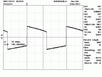
The amplifier was modified with 2.2 nF compensation caps to replace the 3 nF caps used before. I'll be taking some square wave response pictures to domument the effect of this change shortly, and do a frequency response scan when I get back in to work. Currently, the 1625 output tubes are biased at 50 mA apiece. They show no signs of distress at this dissipation level. The next thing I intend to try is to boost the bias to 70mA, as tubelab reported that the small Edcor transformers sound better with more bias. We'll see....
The amplifier was modified with 2.2 nF compensation caps to replace the 3 nF caps used before. I'll be taking some square wave response pictures to domument the effect of this change shortly, and do a frequency response scan when I get back in to work. Currently, the 1625 output tubes are biased at 50 mA apiece. They show no signs of distress at this dissipation level. The next thing I intend to try is to boost the bias to 70mA, as tubelab reported that the small Edcor transformers sound better with more bias. We'll see....
Attachments
- Status
- This old topic is closed. If you want to reopen this topic, contact a moderator using the "Report Post" button.
- Home
- Amplifiers
- Tubes / Valves
- "Shrine" SE Amp using 6AH6 and 1625