Hello everyone,
I am writing in this forum to seek assistance with an issue I have encountered.
Recently, I acquired an SA-9900 amplifier—a machine that, in my opinion, is exceptionally well-crafted and reminiscent of a bygone era.
Unfortunately, there were some burnt output transistors and other damaged transistors on the final amplifier board (AWH037).
To ensure a lasting repair, I proceeded to replace all the transistors on this board. Since many of the original transistors are no longer available, I opted for equivalent replacements—choosing transistors with equal or superior parameters, such as hFE, maximum VCE, and VBE.
Now that the repair work is complete, the sound output is fundamentally correct.
However, I’ve encountered a problem: after some time of the amplifier being powered on, the protection circuit automatically triggers (the relay disconnects the speaker connections). Usually, after a few seconds, it reactivates.
I conducted some measurements and observed that the bias current, initially set on the amplifier, gradually decreases over time. When I measure the voltage between PIN 2 and 6 (as indicated in the service manual), I notice that the values drop from the initial 50 mV calibration to around 10 mV and occasionally even to 0 (at which point the protection intervenes).
Additionally, the initial calibration process is quite challenging because the values read on the tester (both for zeroing the output voltage and for bias current) appear highly unstable. A slight adjustment of the trimmer causes the measured voltage to deviate significantly from the initial value, eventually settling after 1 or 2 seconds.
I wonder if the choice of transistors (or a specific one) has influenced this somewhat erratic behavior, both in the biasing current and in the protection circuit.
Any help is more than appreciated !
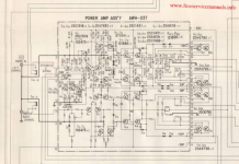
Attached is the schematic diagram of the main amplifier board.
Thank you in advance,
Alberto
I am writing in this forum to seek assistance with an issue I have encountered.
Recently, I acquired an SA-9900 amplifier—a machine that, in my opinion, is exceptionally well-crafted and reminiscent of a bygone era.
Unfortunately, there were some burnt output transistors and other damaged transistors on the final amplifier board (AWH037).
To ensure a lasting repair, I proceeded to replace all the transistors on this board. Since many of the original transistors are no longer available, I opted for equivalent replacements—choosing transistors with equal or superior parameters, such as hFE, maximum VCE, and VBE.
Now that the repair work is complete, the sound output is fundamentally correct.
However, I’ve encountered a problem: after some time of the amplifier being powered on, the protection circuit automatically triggers (the relay disconnects the speaker connections). Usually, after a few seconds, it reactivates.
I conducted some measurements and observed that the bias current, initially set on the amplifier, gradually decreases over time. When I measure the voltage between PIN 2 and 6 (as indicated in the service manual), I notice that the values drop from the initial 50 mV calibration to around 10 mV and occasionally even to 0 (at which point the protection intervenes).
Additionally, the initial calibration process is quite challenging because the values read on the tester (both for zeroing the output voltage and for bias current) appear highly unstable. A slight adjustment of the trimmer causes the measured voltage to deviate significantly from the initial value, eventually settling after 1 or 2 seconds.
I wonder if the choice of transistors (or a specific one) has influenced this somewhat erratic behavior, both in the biasing current and in the protection circuit.
Any help is more than appreciated !
Attached is the schematic diagram of the main amplifier board.
Thank you in advance,
Alberto
Attachments
A few things
When you adjust the dc offset, do so with no signal at the input. Each adjust requires some time to settle. You can use a scope, set for dc coupling and min mV/div setting to see it instead of a dmm
As for the output stage bias, initially set it for spec and as the heatsinks warmup readjust the pot to bring it back to spec. It should stabilize after the warm up period.
As for the protection relay de-energizing, it will do so if there is excessive dc at the output or if there is an over current condition or at turn on and off or the circuit is malfunctions. Need to check the protection ckt dc voltages against the schematic. If they are using 0.22uF blue ecaps, change them to 0.22uF/63V film with 5mm lead spacings
Good luck

Hello everyone,
I am still facing the problem I have reported in this thread.
I had a chance to carry out the calibration as indicated by Rsavas.
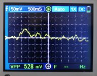
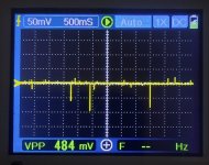
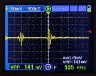
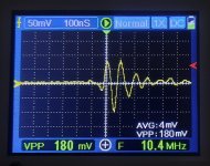
I have attached four photographs showing the voltage at the output of one channel of the amplifier (50 mV / div):
Above all, at this point, how can I eliminate these self-oscillations ?
Thank you in advance to everyone who can help me out.
Alberto
I am still facing the problem I have reported in this thread.
I had a chance to carry out the calibration as indicated by Rsavas.
I have attached four photographs showing the voltage at the output of one channel of the amplifier (50 mV / div):
- the first with a time base of 500 mS with the amplifier switched on not too long ago. The trend is a bit unstable.
- the second again with a time base of 500 mS after a long time since the amplifier was switched on. Spikes can be seen.
- the third with time base 500 nS: it shows some oscillations which then disappear
- the fourth with time base 100 nS: you can see the detail of the oscillation (which is around 10 Mhz frequency).
Above all, at this point, how can I eliminate these self-oscillations ?
Thank you in advance to everyone who can help me out.
Alberto
Attachments
I've attached a PDF of the schematic that seems a bit clearer.
I'm not familiar with the suppliers you've used. Are they trusted to not send counterfeit parts?
Thank you for the scope photos. Be sure to use x10 scope probes--- x1 probe load capacitance can provoke oscillation, especially at internal nodes within an amplifier.
I wouldn't describe scope the waveforms as an oscillation. To my eyes, they look like random noise, clicks, and pops rather than a steady-stage oscillation. Do they sound erratic and like "static"? Any comments?
I suggest testing with an expendable speaker and install a 100 ohm resistor in series to avoid possible damage. Then you can connect speaker+resistor ahead of the protection relay and hear what's happening without intervention of protection circuit.
I surmise there are similar problems in both channels? Are they independent of each other? i.e. if you had stereo speakers, are there independent noises in the two channels?
Is there mechanical susceptibility? Try prodding and tapping with a wooden chopstick or similar tool. It's possible there could be intermittent connections, or the problem can be entirely electronic. Leaky transistors are a notorious mechanism for erratic noise, but other parts are suspect too.
Since you mentioned erratic bias current behavior, you might consider the STV3H diodes. An interesting link:
https://audiokarma.org/forums/index.php?threads/replacing-the-stv-3h-and-4h-diodes.279530/
Replacing the current adjust pot may be wise or at least cleaning it. If the pot's wiper connection is intermittent, the bias current might spike dramatically higher--- scary. If bias current varies slowly and with temperature, perhaps it's not the issue. Be sure to check bias current with no load.
Did you keep the old parts?
If you become convinced a noisy offset voltage is the chief problem, I have an untried experiment we can discuss.
Good luck!
Attachments
It seems that your problem is directly related to the idle current drift. I.e. when the voltage over emitter resistor drops to zero the relay gets activated.I conducted some measurements and observed that the bias current, initially set on the amplifier, gradually decreases over time. When I measure the voltage between PIN 2 and 6 (as indicated in the service manual), I notice that the values drop from the initial 50 mV calibration to around 10 mV and occasionally even to 0 (at which point the protection intervenes).
So you should find the cause of that drift.
I would hook up DMMs to the bases of the driver transistors set Q13/15/17/19 (and their equivalents in the other channel) to see if and how DC drifts there when the output current drifts.
If the voltages do not drift then I would measure voltages ofver the base resistors to see if currents drift.
This is a similar situation to the one that motivated me to create my own "DMM-rig" - did not cost too much but gives one glance overview of the real time situation developments (one could even set up a time lapse camera to record the process):
Last edited:
At first I would like to thank all you guys helping me with this issue.
This is a very supportive community where competent people are providing very useful help.
This is a very supportive community where competent people are providing very useful help.
I've attached a PDF of the schematic that seems a bit clearer.
I do trust them, they are European suppliers with good reputation (Reichelt from Germany while TME is based in Poland). No reason to believe they sell rubbish.I'm not familiar with the suppliers you've used. Are they trusted to not send counterfeit parts?
There is nothing bad I hear from the loadspeakers, just the scope reports a periodic Mhz small oscillation.Thank you for the scope photos. Be sure to use x10 scope probes--- x1 probe load capacitance can provoke oscillation, especially at internal nodes within an amplifier.
I wouldn't describe scope the waveforms as an oscillation. To my eyes, they look like random noise, clicks, and pops rather than a steady-stage oscillation. Do they sound erratic and like "static"? Any comments?
I have already connected them. Good sound from loadspeakers till the protection relais breaks the circuit.I suggest testing with an expendable speaker and install a 100 ohm resistor in series to avoid possible damage. Then you can connect speaker+resistor ahead of the protection relay and hear what's happening without intervention of protection circuit.
The idling current behavour is really similar on both channels.I surmise there are similar problems in both channels? Are they independent of each other? i.e. if you had stereo speakers, are there independent noises in the two channels?
No change if I make the board vibrate (and I refreshed almost all solder points some motnhs ago).Is there mechanical susceptibility? Try prodding and tapping with a wooden chopstick or similar tool. It's possible there could be intermittent connections, or the problem can be entirely electronic. Leaky transistors are a notorious mechanism for erratic noise, but other parts are suspect too.
Very interesting post (the one related to STV3H). They are located in the same heat sink with the transistors driving the very final stage. This heat sink becomes hot to a certain temperature, but I can still keep fingers on it; this happens even without any signal being played; I suppose it is normal). I cleaned the voltage and current regulation trimmers (one of them has been replaced with a multiround one. I do not see any difference between channels though.Since you mentioned erratic bias current behavior, you might consider the STV3H diodes. An interesting link:
https://audiokarma.org/forums/index.php?threads/replacing-the-stv-3h-and-4h-diodes.279530/
Replacing the current adjust pot may be wise or at least cleaning it. If the pot's wiper connection is intermittent, the bias current might spike dramatically higher--- scary. If bias current varies slowly and with temperature, perhaps it's not the issue. Be sure to check bias current with no load.
I did but some of them are in a very bad shape, rusty terminals covered with black matter.Did you keep the old parts?
Ok, thank you so much for your suggestions.If you become convinced a noisy offset voltage is the chief problem, I have an untried experiment we can discuss.
Good luck!
In regards to what Madis64 posted:
"It seems that your problem is directly related to the idle current drift. I.e. when the voltage over emitter resistor drops to zero the relay gets activated.
So you should find the cause of that drift.
I would hook up DMMs to the bases of the driver transistors set Q13/15/17/19 (and their equivalents in the other channel) to see if and how DC drifts there when the output current drifts.
If the voltages do not drift then I would measure voltages ofver the base resistors to see if currents drift.
This is a similar situation to the one that motivated me to create my own "DMM-rig" - did not cost too much but gives one glance overview of the real time situation developments (one could even set up a time lapse camera to record the process):"
I totally agree ... I noticed that the relay breaks the circuit when the idling current drops to 0.
Very interesting approach the one of DMM-rig.
I will do it (maybe one channel at a time to reduce the number of DMM required ...).
As almost all of the transistors were replaced while STV3H are the original ones, do you think that these diodes can have a role in the issue I am facing ?
Thank you so much.
A.
Restating/summarizing a bit: if I interpret correctly, first pic in post 3 shows more than 500mV voltage noise; there's complaint of both erratic offset voltage and bias current, and adjustments are very problematic, perhaps "twitchy."
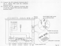
I suspect more than a single problem, but I take issue with the prescribed adjustment procedure in the service manual page 20, pasted below:


I'm ambivalent about having a 8 ohm load present during offset adjustment (don't think it matters much), but believe a load should not be present during bias current adjustment. I contend that bias current adjustment is establishing the Class A bias current is the crossover region and is setting the current flowing between the positive and negative output transistors; with a load present, any offset errors divert current into the load and corrupt the sensed bias current being monitored at the test points. Without a load, bias current and offset voltage should be largely independent.
Try trimming bias current without a load and see if adjustability improves. Without a load, does tendency toward protection trigger lessen? I think it may be helpful to disable protection sensing of voltage faults; then swap and sense voltage but suppress current sensing.
I suspect more than a single problem, but I take issue with the prescribed adjustment procedure in the service manual page 20, pasted below:
I'm ambivalent about having a 8 ohm load present during offset adjustment (don't think it matters much), but believe a load should not be present during bias current adjustment. I contend that bias current adjustment is establishing the Class A bias current is the crossover region and is setting the current flowing between the positive and negative output transistors; with a load present, any offset errors divert current into the load and corrupt the sensed bias current being monitored at the test points. Without a load, bias current and offset voltage should be largely independent.
Try trimming bias current without a load and see if adjustability improves. Without a load, does tendency toward protection trigger lessen? I think it may be helpful to disable protection sensing of voltage faults; then swap and sense voltage but suppress current sensing.
Attachments
Last edited:
I am not an expert in these diodes but some diodes are called suicidal and then again these folks think that they do not fail:while STV3H are the original ones, do you think that these diodes can have a role in the issue I am facing ?
https://audiokarma.org/forums/index.php?threads/sanken-stv3h-y-testing-and-installation.822754/
Measuring and monitoring base voltages on Q13/15 should give you a clue of their performance.
- Home
- Amplifiers
- Solid State
- SA-9900 protection circuit / biasing problem