D
Deleted member 148505
D
Deleted member 148505
I see. It is a bit too close for R!3,14 so perhaps the Japanese style, radial lead ceramic box type would be better. 'Not sure what you mean about the input being closer to the output now. Could you point this out?
The speaker output is nearer the input stages of the amplifier...
D
Deleted member 148505
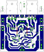
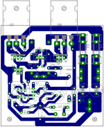
Hmm.. The second version has promise - the output stage tracks are commendably short in both. Perhaps reducing the trace length for the power input connections right back to minimum distance from the fuse holder (keep the place for the caps) would reduce input exposure to switching EMR. There appears to be room to extend the ground tracks to the decoupling caps and move them up too, as you don't need that big output connection pad.
My view is that the less and shorter power tracks on the PCB, the better. If that means removing the big hardware bits that do nothing good, like the spade connectors, then remove them, because leads can always be disconnected at the PSU end. I realise it is a DIY convention to fit connectors but I don't see any point duplicating them at every connection.
My view is that the less and shorter power tracks on the PCB, the better. If that means removing the big hardware bits that do nothing good, like the spade connectors, then remove them, because leads can always be disconnected at the PSU end. I realise it is a DIY convention to fit connectors but I don't see any point duplicating them at every connection.
D
Deleted member 148505
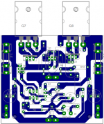
Now if you moved the supply input Power Ground up to the decoupling ground you could them completely delete the two edges of the PCB and delete that U shaped ground trace. Bring in the +ve & -ve Power input next to the decoupling ground. The PCB would end up being about 15mm narrower and all the High Current traces would all be at the output device side/end.
D
Deleted member 148505
Now if you moved the supply input Power Ground up to the decoupling ground you could them completely delete the two edges of the PCB and delete that U shaped ground trace. Bring in the +ve & -ve Power input next to the decoupling ground. The PCB would end up being about 15mm narrower and all the High Current traces would all be at the output device side/end.
Like in the original p3a pcb...
Is the power ground contributes to noise in its surrounding areas?
Thanks
Every circuit has a current that gets sent out and this MUST return to the beginning. If you arrange that circuit so that it is a flow and return pair then it becomes resistant to receiving interference and it emits less interference.
In a cable this is often achieved by running a twisted pair. In a 3wire PSU +ve, -ve & Zero Volts this would be a twisted triplet.
On a PCB the flow and return traces would be laid out as a pair. Either next to each other or or on adjacent sides of a multilayer PCB.
This Flow and Return pair can be applied to every circuit.
The Power Supply is one circuit. The output devices and the decoupling is another circuit. The output devices and the SPKR out and SPKR Return is another circuit, the Signal Input and Signal Return is another circuit.
Some of your PCB circuits are laid out for minimising that interference, either in or out. But your PSU circuit is spread around the PCB and will emit interference that could be picked up by the other circuits on the PCB or even in an adjacent PCB.
to be honest with you i write this without following what happen with the post so far ..
check this ..
If one before starting to design a pcb specify a list of rules to be kept while designing the pcb eventually will realize that many of the rules conflict with each other and if you want to ""keep""the one rule will loose the other
many of the problems that will occur might be solved with a double sided pcb but then you need to be ready to walk in the induction and capacitance path that will be formatted from the layers and traces of pcb
so after all this an endless game the all trick is to find or categorize which of these rules you need to keep more and probably work with elimination process
It can never be such a perfect pcb or a perfect amplifier ...each and every of the given pcbs will work and produce music problem is that the depth of detail we are looking at often is barely audible or measurable but still will add something to a working amplifier...
D
Deleted member 148505
you cant measure a pcb ...it has to be made from experience and careful choice of the rules we talked above .
When finished you measure the amp and to find out the total result if problems show up simply redesign the pcb and do it all over again
in more than 4 years i designed and tested almost 12 different pcb to end up with one that meats my needs regarding size dimension and sound qualities
When finished you measure the amp and to find out the total result if problems show up simply redesign the pcb and do it all over again
in more than 4 years i designed and tested almost 12 different pcb to end up with one that meats my needs regarding size dimension and sound qualities
So I guess I just have to be contented with the current pcb... and just revise later if the measurements suck...
BTW what are the measurements that tell that the pcb layout is excellent?
Thanks
There are no empirical measurements for excellence. If you amp is immune to conducted or radiated electromagnetic interference between DC and DAYLIGHT then your layout is basically okay.
I may be wrong but I have yet to see an audio component that has been subjected or complies with any EMI regulation.
D
Deleted member 148505
you cant measure a pcb ...it has to be made from experience and careful choice of the rules we talked above .
When finished you measure the amp and to find out the total result if problems show up simply redesign the pcb and do it all over again
in more than 4 years i designed and tested almost 12 different pcb to end up with one that meats my needs regarding size dimension and sound qualities
Yes what I meant was the measurement of amplifier's performance given the pcb layout...
I'll try the second version of the layout, and if I won't find any oscillation problems then I'm ok with it
")
Can you suggest on how to test amplifier's stability?
Thanks
Last edited by a moderator:
D
Deleted member 148505
There are no empirical measurements for excellence. If you amp is immune to conducted or radiated electromagnetic interference between DC and DAYLIGHT then your layout is basically okay.
I may be wrong but I have yet to see an audio component that has been subjected or complies with any EMI regulation.
What do you mean by daylight? Is it fluorescent lamp?
when you have a standard and a given amount of thd ...you need to be able to notice changes for the best or the worst in the ranges of 5-20% and then to be able to determine if this pcb related
that is a very complicated job requires extremely sophisticated equipment in order to achieve perfection keep in mind that often the measured issues are not even audible ...
It is obvious that this all talk is about milking a mosquito or its about the definition of the word perfect ...
that is a very complicated job requires extremely sophisticated equipment in order to achieve perfection keep in mind that often the measured issues are not even audible ...
It is obvious that this all talk is about milking a mosquito or its about the definition of the word perfect ...
D
Deleted member 148505
- Home
- Amplifiers
- Solid State
- Rod Elliot P3A Layout - Critics