Hi Roender,
I have had a good look at your design and consider it seminal. This is one of the most elegant designs I've seen on the web.
DIY is a difficult environment, and you may receive some criticism, particularly over your comments that Q15-Q16 have a gain of one, but I give credit for an outstanding design and salute your efforts.
As I see it, input is an 'ultralinear' cascode, where the bias point of the cascode devices, Q21/18, is at the same AC potential as the sources of the input devices. I've used this approach, it works very well, and it means that the voltage across each of the input jfets is constant. Thus, the current output which flows to the emitters of Q14 and Q16 is controlled utterly by transconductance changes within the input devices. That is, a differential voltage input leads to a pure differential current output - a transconductance amplifier.
However, your second stage takes this current output and transforms it into a voltage output at the collector of Q16. As I understand it, this is a transresistance amplifier, where the concept of voltage gain is not strictly relevant. The flashes of brilliance here are the elegant current sources at Q11/Q13 using the same voltage reference, the constant voltage between the bases of Q11/13 and Q14/16, and the very stiff current mirror at Q6/7/15. These blocks would ensure incredibly high OLG, and you've verified this at 94dB, which is higher than almost any other audio power amp I've seen.
Compensation is always the clincher. You've done it with a couple of 15pF caps to ground off the collectors of Q15/16. Did you try it across the collectors of Q18/21, and did you consider phase lead from Q15/16 collectors back to the feedback node? It's always tricky to decide, and the sonics depend greatly on the regime you decide to use.
A brilliant design, Roender. My congratulations!
Cheers,
Hugh
AKSA said:Hi Roender,
Compensation is always the clincher. You've done it with a couple of 15pF caps to ground off the collectors of Q15/16. Did you try it across the collectors of Q18/21, and did you consider phase lead from Q15/16 collectors back to the feedback node? It's always tricky to decide, and the sonics depend greatly on the regime you decide to use.
Mr. Dean,
Compensation method is not a big problem in a folded cascode topology.
I've try that, from collectors of q15/16 to gnd, and it sound a little bit bright.
I will try the other method, phase lead, and I'll report back here the results
Thank you
Mihai RAUTA
AKSA said:
... did you consider phase lead from Q15/16 collectors back to the feedback node?
Hugh
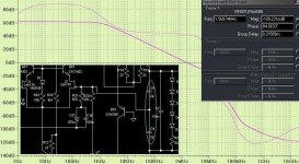
This looks very promising, at least in simulator. More phase margin (+20grd) and more SR too, because now "VAS" is loaded only by the output stage. With only 2 x 2pF, good ...
It seems that in this case I can drop output coil ... very good

Thank You
Attachments
Hi Mihai,
My pleasure, it is always very satisfying to an old fellow like me to see talented young designers who see things much as I see them...... of course this is ego on my part, I freely admit.
I did not mention the marvellous way you have stacked the voltage reference LEDs - no less than 5!!! You must have been thinking of Christmas when you did this, but it's very economical design (although I have my doubts Q8 is needed....) and I like it!
LEDs in audio amplifiers are a wonderful way to see if it is working.... there is nothing quite like a visible sign when working at the test bench. I love LEDs, they are cheap, quiet, and very stable.
I do have some comments about the Q15/16 collector drive to the output stage, however. It's very high impedance, and with the varying load seen at Q19/20 there will be some variation in OLG, though nothing like as much as if Q1 and Q3 were missing and it was a simple Double Emitter Follower. Variation in OLG with loading, particularly around the crossover region when transistors turn on and off, is problematic and where much of the low level spatial information is lost. Your output triple is good, but I'd try replacing Q1/Q3 with low current, thermally robust mosfets, say IRF710 series, and then you could use TO92 devices for Q19 and Q20 and drop the collector current to 1.5mA, making them easier to drive. Because of the gate capacitance of these mosfets, the drive current would eventually meet with SR issues, and this would have the effect of pulling back OLG at higher frequencies, in turn enhancing stability.
I admit I'm just giving my thoughts off the top of my head, without PSpice. From the stability POV, PSpice is not very reliable, but nothing can substitute the mental arithmetic of figuring out all the currents and voltages in your head.
The advantage of phase lead, Mihai, is that it means you can reduce toxic lag compensation slightly, and it will improve tolerance to reactive loading at the speaker.
Mihai, you can use just one phase lead cap, say around 3pF, from collector of the active device, Q16, back to fb node, and back it up with roughly 10pF of lag comp from collector Q16 to ground.
Guillermo,
This is a very clever, well thought out circuit. It shows quite a mastery of circuit topology, at least from my POV. The challenge would be to achieve the same performance with less components. I think it can be done, but if you built this circuit it would sound very, very good with very low intermodulation. But much of the sonics derive from the compensation used; it's very, very important and not evident from the topology.
The output stage would have reasonable bias stability but it could be improved with 0R33 emitter resistors. The charge suckout mechanism might need some tweaking; I'd be surprised if the cap is large enough; I'd go for around 1uF, and trim the resistor for best sonics. I don't believe 77mA is needed, however, as the drivers are always on anyway.
Cheers,
Hugh
How about omitting the cascode transistor, Q10 (2sa1360), and adding an additional diode-connected transistor 2sc3423 in the current mirror (making it a 4-transistor Wilson current mirror)? Q14 is common-base, and has high enough output impedance at the collector already - definitely enough to drive the 4-transistor Wilson current mirror. Q14 will continue to operate at constant collector-base voltage.
It probably makes no difference to the sonics, but it will look more beautiful and mirror-symmetric, and more transistors can be bought in pairs rather than having to buy one extra oddball PNP for the Q10 cascode.
It probably makes no difference to the sonics, but it will look more beautiful and mirror-symmetric, and more transistors can be bought in pairs rather than having to buy one extra oddball PNP for the Q10 cascode.
linuxguru said:How about omitting the cascode transistor, Q10 (2sa1360), and adding an additional diode-connected transistor 2sc3423 in the current mirror (making it a 4-transistor Wilson current mirror)? Q14 is common-base, and has high enough output impedance at the collector already - definitely enough to drive the 4-transistor Wilson current mirror. Q14 will continue to operate at constant collector-base voltage.
It probably makes no difference to the sonics, but it will look more beautiful and mirror-symmetric, and more transistors can be bought in pairs rather than having to buy one extra oddball PNP for the Q10 cascode.
In your proposed architecture, Q14 will dissipate twice power as it is now. Not good for second stage thermal balance.
>In your proposed architecture, Q14 will dissipate twice power as it is now. Not good for second stage thermal balance.
Agreed - so keep Q10 to halve Q14 collector voltage to maintain thermal balance between Q14/Q16, and add another NPN 2sc3423 diode-connected transistor in the current mirror to make it into a 4-transistor Wilson current-mirror. It can't hurt, and it will look more symmetric.
Agreed - so keep Q10 to halve Q14 collector voltage to maintain thermal balance between Q14/Q16, and add another NPN 2sc3423 diode-connected transistor in the current mirror to make it into a 4-transistor Wilson current-mirror. It can't hurt, and it will look more symmetric.
Also - any alternative to R29 for maintaining constant drain-source voltage on the input JFETs? I'm thinking about the thermal noise in R29, which is coupled from the bases of Q21/Q18 to sources of J1/J2. This is common-mode, so it's not a severe issue, but it would be nice to minimize it anyway.
How about:
a) Bypassing R29 with a suitable cap?
b) Substituting a zener instead of R29?
c) Substituting a Vbe multiplier instead of R29?
d) Substituting a band-gap reference like TL431 instead of R29?
How about:
a) Bypassing R29 with a suitable cap?
b) Substituting a zener instead of R29?
c) Substituting a Vbe multiplier instead of R29?
d) Substituting a band-gap reference like TL431 instead of R29?
AKSA said:Hi Mihai,
1. ... although I have my doubts Q8 is needed....
2. ... I do have some comments about the Q15/16 collector drive to the output stage, however. It's very high impedance, and with the varying load seen at Q19/20 there will be some variation in OLG, though nothing like as much as if Q1 and Q3 were missing and it was a simple Double Emitter Follower. Variation in OLG with loading, particularly around the crossover region when transistors turn on and off, is problematic and where much of the low level spatial information is lost.
3. ... The advantage of phase lead, Mihai, is that it means you can reduce toxic lag compensation slightly, and it will improve tolerance to reactive loading at the speaker.
4. ... The output stage would have reasonable bias stability but it could be improved with 0R33 emitter resistors. The charge suckout mechanism might need some tweaking; I'd be surprised if the cap is large enough; I'd go for around 1uF, and trim the resistor for best sonics. I don't believe 77mA is needed, however, as the drivers are always on anyway.
Cheers,
Hugh
Mr. Dean,
Thank you again for your good advice regarding PL compensation method.
Respectfully allow me to not entirely agree with you.
1. Q8 is there to isolate outside signals to reach active current source transistor. In that way, will be hard to modulate output CCS current.
I know that there is not much voltage variation at Q8 collector but in any case Q8 will not do any harm to sound fingerprint.
2. The output stage has a input impedance in the Mohm order. At 20Kz, near full output power, Q19/Q20 base currents variation is in the range of 9 to 24uA
3. What is the difference, in sonic fingerprint, between PL and lag compensation?. With PL, if there is enough phase margin - let say more than 80grd, can I omit output coil?
4. Well, the 77mA drivers current has no magic in it as number but the MJE15034/15035 drivers are more linear at this collector current. I've read somewhere, now I don't remember where, that carriers in base output transistors will be much faster evacuated, at reverse bias, if driver current is a little bit higher than normally required for proper driver classA operation. I could be wrong in that ...
As per suckout capacitor, I don't have any experience with it regarding sonic signature.
The 0.1ohm Re resistors are not to small because output transistors are matched at less than 5% hfe. All 0302/0281 ONsemi transistors are factory matched in 10% hfe between 50mA to 5A Ic.
I need a small as possible Re in order to achieve as much as possible class A operation, without overbiassing output stage and to have a smooth transition between A and B operation class.
The bias current is very stiff and time stable because all output transistors are on the same heatsink and all are at the same TC with NJL diodes incorporated in output transistors.
Mihai
linuxguru said:Also - any alternative to R29 for maintaining constant drain-source voltage on the input JFETs? I'm thinking about the thermal noise in R29, which is coupled from the bases of Q21/Q18 to sources of J1/J2. This is common-mode, so it's not a severe issue, but it would be nice to minimize it anyway.
How about:
a) Bypassing R29 with a suitable cap?
b) Substituting a zener instead of R29?
c) Substituting a Vbe multiplier instead of R29?
d) Substituting a band-gap reference like TL431 instead of R29?
Noise is not a problem there because will be rejected by LTP CM.
There is no need for a low impedance in transistors bases of common base topology. What do you know about Colpitts oscillator?
HI Mihai,
Of course! I would be disappointed if you did not - motivation comes from within, not from without.....
Modulation of the output CCS current will be asymmetrical, leading to even order distortion. This is benign, and would scarcely amount to 0.0001% anyway. You would need to replace Q9 with the 3423, however, for increased dissipation.
My mistake. This is more than acceptable, and vindicates your choice of the output triple. The CFP driver stage indeed has hugely high Zin, and this should preserve low level control over the outputs beautifully.
Phase lead has less effect on SR and appears much more benign than LC. You need some LC, and in my opinion you will still need an output coil (<1uH) to prevent ingress of RFI, but LC could be reduced to maybe two thirds of that presently used alone with a tiny amount of PL. The effect on the sonics of reduced LC is very positive, and the PL makes it then unconditionally stable.
The linearity of a CFP in Class A is essentially dominated by the master, not the slave device. I say Class A because even at high peak currents, the inactive side driver will still be on at all times because of R5. The real challenge is to sharply control the switching of the output devices. Since the master, Q19/20, is in constant 3mA current, the high levels of local fb will render the transfer function of the slave, Q1/3, almost insignificant, that is why I recommend a mosfet here. You could try a lower driver current in simulation; you might find the linearity is not much affected. In any event, changing this current is merely a change in R5, so it's easy to check sonically as well. In truth, the linearity of the output stage will be largely dominated by the variations in Vbe of the output devices (non-ohmic) and the ohmic losses of the emitter resistors.
I do like your output stage. I think it's very cool.
Mihai, do experiment with the suckout cap. It's very important to the sonics, and should have low dielectric absorption.
On output matching, what is the variation of stage current on each conjugate pair? I use 0R47 emitter resistors, match my beta within 2% and Vbe within 1mV, and achieve better than 3% matching between output pair stage currents.
I'll say it again; these are not criticisms, merely discussion points, I LOVE this design.
Cheers,
Hugh
Respectfully allow me to not entirely agree with you.
Of course! I would be disappointed if you did not - motivation comes from within, not from without.....
1. Q8 is there to isolate outside signals to reach active current source transistor. In that way, will be hard to modulate output CCS current.
Modulation of the output CCS current will be asymmetrical, leading to even order distortion. This is benign, and would scarcely amount to 0.0001% anyway. You would need to replace Q9 with the 3423, however, for increased dissipation.
2. The output stage has a input impedance in the Mohm order. At 20Kz, near full output power, Q19/Q20 base currents variation is in the range of 9 to 24uA
My mistake. This is more than acceptable, and vindicates your choice of the output triple. The CFP driver stage indeed has hugely high Zin, and this should preserve low level control over the outputs beautifully.
3. What is the difference, in sonic fingerprint, between PL and lag compensation?. With PL, if there is enough phase margin - let say more than 80grd, can I omit output coil?
Phase lead has less effect on SR and appears much more benign than LC. You need some LC, and in my opinion you will still need an output coil (<1uH) to prevent ingress of RFI, but LC could be reduced to maybe two thirds of that presently used alone with a tiny amount of PL. The effect on the sonics of reduced LC is very positive, and the PL makes it then unconditionally stable.
4. Well, the 77mA drivers current has no magic in it as number but the MJE15034/15035 drivers are more linear at this collector current. I've read somewhere, now I don't remember where, that carriers in base output transistors will be much faster evacuated, at reverse bias, if driver current is a little bit higher than normally required for proper driver classA operation.
The linearity of a CFP in Class A is essentially dominated by the master, not the slave device. I say Class A because even at high peak currents, the inactive side driver will still be on at all times because of R5. The real challenge is to sharply control the switching of the output devices. Since the master, Q19/20, is in constant 3mA current, the high levels of local fb will render the transfer function of the slave, Q1/3, almost insignificant, that is why I recommend a mosfet here. You could try a lower driver current in simulation; you might find the linearity is not much affected. In any event, changing this current is merely a change in R5, so it's easy to check sonically as well. In truth, the linearity of the output stage will be largely dominated by the variations in Vbe of the output devices (non-ohmic) and the ohmic losses of the emitter resistors.
I do like your output stage. I think it's very cool.
Mihai, do experiment with the suckout cap. It's very important to the sonics, and should have low dielectric absorption.
On output matching, what is the variation of stage current on each conjugate pair? I use 0R47 emitter resistors, match my beta within 2% and Vbe within 1mV, and achieve better than 3% matching between output pair stage currents.
I'll say it again; these are not criticisms, merely discussion points, I LOVE this design.
Cheers,
Hugh
AKSA said:HI Mihai,
On output matching, what is the variation of stage current on each conjugate pair? I use 0R47 emitter resistors, match my beta within 2% and Vbe within 1mV, and achieve better than 3% matching between output pair stage currents.
Cheers,
Hugh
Dear Mr. Dean
The matching was made at 100mA Ic and 20V Vce. The following transistors was selected from a lot of 15 peers
NJL0281 [npn] NJL0302 [pnp]
-----------------------------------------------
hfe Vbe[mV] hfe Vbe[mV]
-----------------------------------------------
138 593 133 600
136 592 133 600
134 592 133 600
-----------------------------------------------
132 594 129 600
128 594 129 600
129 594 128 600
The current imbalance is under 8% at idle, but I'm not so sure that I can measure that precisely because I have not access to both Re pins due to PCB layout. If I move the probe only 5mm along tick Re resistor pin, the measured Vre value change in the range of 0.2 to 0.5mV.
Best regards,
Mihai RAUTA
- Home
- Amplifiers
- Solid State
- RMI-FC100, a single stage audio power amplifier