Will the Saphire 4.1m circuit safely handle the higher voltages of 15V?
The Sapphire amplifier circuit itself can be run at higher supply rails, scaling R7,8 in proportion to the voltage increase to keep the bias currents constant.
The Sapphire 4.1m boards are set up for 12 VAC transformer secondaries however, giving +/- 18 V rectified DC with internal regulation to generate 11 V and -11 V rails. Several adjustments are needed to change the circuit to run with 15 VAC secondaries and higher internal voltage rails: The voltage rating of the filter caps, the Zener voltage, and R7,8.
I've read in the datasheets (plus in my own measurement findings) that higher rail volts equate to lower THD.
It's true. The smaller the signal voltage and the greater the power supply voltage, the lower the distortion.
But as always things are not so simple. The smaller the signal current and the greater the device bias current, the lower the distortion.
And, for a given thermal envelope, you have to choose between more voltage or more bias current, since P=VI.
/R
I'm quite pleased with my Saphire amplifier, it really sings.
As I already mentioned, I decided to use stabilized power supply from two cascaded LT317 regulators and it proved to be good decision. Load regulation is excellent which allow very low offset - practically offset is only associated with temperature variations, while the power supply noise is very low.
Now, after a while, I think I can do better than that. On PCB there is already place for zener regulator - since I don't actually need load regulation, I can use it, but without the zener diode, simpply converting it to a simple capacitance multiplier, where Q16 is isolating filter capacitor C6 from the load, making the capacitor value appear to be multipled by the beta of the transistor.
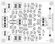
The change for the schematic is very simple: R21 - simple junction, D1 - good place to put 100nF MKT capacitor, R23 1k should be OK, C6 - 47uF tantalum, could be bigger but I don't have bigger value and it definitely should be either film on tantalum for the gyrator to work best.
The forward voltage drop across the Q16 transistor should be roughly [0.7v + (Ic/hfe)*R1], so only about 1.7V which should not rise heat-sink (common with the output transistors) temperature significantly. I will increase my regulators output by this value.
I had independent little heat-sinks installed, but changed it to one common one - it helped a bit to limit offset drift for both channels - there is no temperature compensation so offset can be set to zero while iddle, but it will rise during listening - using 1kHz sine wave signal with maximum power (resistance load 32ohm) the offset jumps from 0mV to max 60mV, while with normal listening levels it is max +/- 10mV. While idle, the transistors temperature goes down.
I'm using little more voltage +/-12V as I set up external regulator for 12V, and in your original design there is 0,7V voltage drop after the zener so mine rails have little more voltage.
I were listening the amp with bias in the range 40-100mA but the is not difference that can be noticed. R17 is now 4R7 and for different values of R11 I have voltage drop on R17 as: 220R 0,21V , 330R 0,31V , 470R 047V. With more than 60mA there is too much heat , so I thing I will leave it as 44mA , with default value of R17=220R
For now, all my tests are in open case, maybe the solution is to actually put more bias, generate more heat, and build inside the case stable temperature - 60 degrees on the heat-sink ?
My overall feelings towards this amp are quite positive.
I finally decided to go for closed loop (R3x=2200, and R2: 1k5, 680R 180R) - output impedance is smaller and it better handles different loads , so it easier to build an universal amp, good for both headphones 16, 32 and 300 or 600 ohs.
I'm testing it with Grado SR325 and HD600 and 15db with pot 20K is quite good for both.
As I already mentioned, I decided to use stabilized power supply from two cascaded LT317 regulators and it proved to be good decision. Load regulation is excellent which allow very low offset - practically offset is only associated with temperature variations, while the power supply noise is very low.
Now, after a while, I think I can do better than that. On PCB there is already place for zener regulator - since I don't actually need load regulation, I can use it, but without the zener diode, simpply converting it to a simple capacitance multiplier, where Q16 is isolating filter capacitor C6 from the load, making the capacitor value appear to be multipled by the beta of the transistor.
The change for the schematic is very simple: R21 - simple junction, D1 - good place to put 100nF MKT capacitor, R23 1k should be OK, C6 - 47uF tantalum, could be bigger but I don't have bigger value and it definitely should be either film on tantalum for the gyrator to work best.
The forward voltage drop across the Q16 transistor should be roughly [0.7v + (Ic/hfe)*R1], so only about 1.7V which should not rise heat-sink (common with the output transistors) temperature significantly. I will increase my regulators output by this value.
I had independent little heat-sinks installed, but changed it to one common one - it helped a bit to limit offset drift for both channels - there is no temperature compensation so offset can be set to zero while iddle, but it will rise during listening - using 1kHz sine wave signal with maximum power (resistance load 32ohm) the offset jumps from 0mV to max 60mV, while with normal listening levels it is max +/- 10mV. While idle, the transistors temperature goes down.
I'm using little more voltage +/-12V as I set up external regulator for 12V, and in your original design there is 0,7V voltage drop after the zener so mine rails have little more voltage.
I were listening the amp with bias in the range 40-100mA but the is not difference that can be noticed. R17 is now 4R7 and for different values of R11 I have voltage drop on R17 as: 220R 0,21V , 330R 0,31V , 470R 047V. With more than 60mA there is too much heat , so I thing I will leave it as 44mA , with default value of R17=220R
For now, all my tests are in open case, maybe the solution is to actually put more bias, generate more heat, and build inside the case stable temperature - 60 degrees on the heat-sink ?
My overall feelings towards this amp are quite positive.
I finally decided to go for closed loop (R3x=2200, and R2: 1k5, 680R 180R) - output impedance is smaller and it better handles different loads , so it easier to build an universal amp, good for both headphones 16, 32 and 300 or 600 ohs.
I'm testing it with Grado SR325 and HD600 and 15db with pot 20K is quite good for both.
Attachments
Hi, thanks for the detailed observations.
Reworking the on-board Z-Reg as a capacitance multiplier is a clever idea. Why not? As you say, if the supply is already regulated this is the most efficient use of those components and it will provide additional noise filtering.
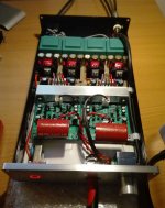
You were lucky to get all the four boards packed into the case. Not a lot of room left...
Anyhow, glad the project came together successfully for you and thanks again for sharing.
Reworking the on-board Z-Reg as a capacitance multiplier is a clever idea. Why not? As you say, if the supply is already regulated this is the most efficient use of those components and it will provide additional noise filtering.
You were lucky to get all the four boards packed into the case. Not a lot of room left...
Anyhow, glad the project came together successfully for you and thanks again for sharing.
I finally decided to go for closed loop (R3x=2200, and R2: 1k5, 680R 180R)
Richard recommends 2.2k for R2 when going closed loop.
Why do you have 3 different values(1.5k, 680 and 180 ohms) listed?
It's true. The smaller the signal voltage and the greater the power supply voltage, the lower the distortion.
But as always things are not so simple. The smaller the signal current and the greater the device bias current, the lower the distortion.
And, for a given thermal envelope, you have to choose between more voltage or more bias current, since P=VI.
/R
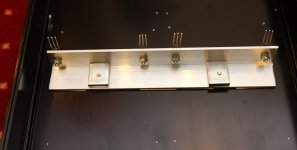
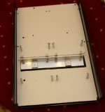
So, having the case made as full aluminium body, I modified the heat sink to get better thermal envelope
")
For the left board I installed capacitance multiplier - voltage drop is 1.20V so I increased the power supply to provide 13,20V to compensate and keep the rails at +/- 12V and installed output transistors on the other side of PCB, transferring heat to the case. The bias is set to 100mV and it has almost no impact on the case temperature - output transistors are barely warm - maybe some kind of thermal resistance layer between heat sink and the case should be installed to let the output transistor work in higher temperature. There is definitely lot of thermal reserve available now to increase both voltage and bias, if anyone want to do so.
For the right board bias is set to 44mA, output transistors just with small heatsinks and power supply directly from the regulated power supply, the rail set to +/- 12V.
Now I need some time to compare the two. I will take the amp to work and give it a trough measurement session with a good equipment that I have available at work.
Of course there is no audible difference between them - I didn't expect any, but surely it should be measurable.
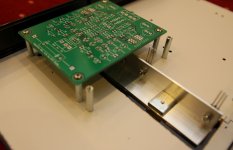
Photos were taken with a second set of PCB, waiting for the second build to come ... just to give the idea how it can be easily done. Once soldered, the board needs to be lifted together with the heat sink, but it is serviceable.
Attachments
That's some nifty metalwork there.
In terms of thermal envelopers, we need to keep in mind that this is a headphone amplifier. Even class A, there are diminishing returns kicking in big time when increasing bias current, especially when paired with high-Z 'phones.
This is because the more bias current, the more work the amp has to do just to drive the output transistors. Eventually this is the limiting factor for the distortion, rather than the headphone load.
, the more work the amp has to do just to drive the output transistors. Eventually this is the limiting factor for the distortion, rather than the headphone load.
True, the total power consumption of the box while idle is about 16W, and since the amp works in class A it is more or less constant no matter what the load the amp is driving.
This is a stationary amp with a large and heavy case (this is actually the same one as you are using - model 1907A from aliexpress) so I think it just right to use it and setting bias of 100mA sounds reasonably to me.
The measurement should be done to actually prove that it make sens to do so.
I have another amp built, based of FETT transistors (Toshiba 2SK200/2SK1529) that is running with 320mA of bias current , still being the headphone amp, and a very good one, with the transformer 80VA
The drawback of employing the case as part of cooling system, is the long time the amp requires to reach stable state.
In terms of DC offset - it starts with 60mV to quickly drop to about 30mV and than very slowly goes towards 0mV. I already did some test with case closed and after about 30-45 min the DC offset is basically non existing and very stable - changing the volume or stressing the amp with resisive load doesn't affect it as there is no more cooling/heating process.
This is only true for the left channel, the right is not as stable and the DC offset drift can be observed. For this alone, I think, it make sense to do the trouble of modifying the cooling.
Playing with the right thermopad installed between the case and the heat sink should mitigate the problem of long time required to reach stable point and should also set the working temperature of the output transistors a bit higher.
At night there is already quite cold here (about 5 degrees last night) so I had a chance to play with changing environment a bit - putting on the window sill to quickly cool down.
The next modification is to add DC-protection and muting while switching ON/OFF the amp and reconnecting the headphones jack and the amp should be announced as DONE.
5 degrees? Wow, we're lucky if it cools to 25 C at night!
(that is not an exaggeration, typical night lows are 26-27)
Anyhow - your offset experiences line up closely with mine: about 50-100 mV on power up, falling to under +/- 15 mV warmed up. I also note there are no audible "thumps" on turn on or turn off, though there is a small wiggle in the output voltage viewed on the 'scope.
I'm having a noise problem, even with the grounded input.
Noise that reminds rain on the roof.
The pcb is out of the enclosure, I have already grounded it directly to the output connector, but I still can not solve it.
ps: R3x=2.2k R2=470
No DC at the output is OK.
AC at around 22mV.
Noise that reminds rain on the roof.
The pcb is out of the enclosure, I have already grounded it directly to the output connector, but I still can not solve it.
ps: R3x=2.2k R2=470
No DC at the output is OK.
AC at around 22mV.
No DC at the output is OK.
AC at around 22mV.
Do you have 22mV AC on the output with no signal on input ?
How do you measure that ?
20 mV AC cannot be acucatley measured by any cheep multimetr, so could be just an error ?
Do you have 22mV AC on the output with no signal on input ?
How do you measure that ?
20 mV AC cannot be acucatley measured by any cheep multimetr, so could be just an error ?
I'm out of scope at the moment.
These measures is what the fluke tells me, sorry.
I can see that this noise does not come from the signal, it is there all the time, can it be some defective transistor or a resistor to the cause?
I used the input from my Profire610 to try to see something.
About -40db, it's quite uncomfortable.
Even with the input directly grounded, without potentiometer.
If you increase the gain setting of R3 and R2 the noise increases slightly. (Currently R3 = 22k R2 = 2.2k)
I tried to make land connections directly at some points because I thought it was similar to the ground loop, but nothing seems to solve, and I could not make things worse either.
The noise is there, and there it stays the same forever.
I'm tired, tomorrow I think better, I did not want to distrust the transistors, but ...
Attachments
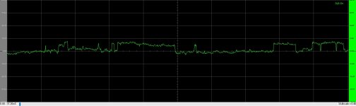
That's an odd one. It looks like a register shift between two stable states.
I'd guess a cracked trace or bad solder joint somewhere forming an intermittent connection.
What are the x and y axis scale on that plot?
Without scope I feel like a blind should feel.
The fact is that by decreasing the gain the noise disappears completely.
I'm testing now with R3x = 2.2k R2 = 1k. And I think this gain factor is enough.
My favorite headphones are Koss PortaPro (60 ohms)
I also have an AKG MKIII (55 ohms), but I like koss more.
And I'm in love with the stereo spectrum, it's airy, awesome!
Ally with very clear treble.
That high gain noise, do not you? Can this be characteristic of cheap transistors?
Best Regards.
One channel or both? This is important.
If you want more gain and still "play it safe", keep R2 as 1k and increase R3x to 4.7k. That's 15 dB, the same as your original setting.
The other thing to try is to add a Zobel filter (47 ohms + 4.7 nF) on the output.
I haven't checked all the D3x configs for stability. I can do that quickly by changing my jumper settings. I'll get back to you with the result. I know already 27 dB is fine. Most everyone else has built the R3 config, so I don't have much field data on the the closed loop build.
It's not the increased gain that causes instability, the CFA circuit design means it's a bit more complicated. Basically, the lower the value of R3X the more problematical things potentially get, and for a given value of R3X the higher the value of R2 the more problematical, so its the lower gain settings listed in the BOM table that are the worry, not the high gain settings.
Last edited:
I just wonder why would someone want so much gain ?
With 2V RMS source (often found in many sources) 13bB provide voltage gain that will cause the amp to hit the voltage rail limit even before half of the volume settings. With input signal 2V RMS , 20k pot, gain set to 15bB and 32 resistive load the cliping starts with about 80% of the maximum volume.
In my amp the rail is slightly higher (+-12V) so I bet that with the default supply from zener reg, clipping starts sooner with Vpeak about 9V or lower. Just before clipping, the amplifier delivers 1,5W into 32 ohm, over 210mA of current which is huge.
I'm curious hot did you calculate the "general recommendation for headphone amplifier circuit gain based on headphone data above" in your excel file, as I found it extremely high.
There is excellent Headphone Power Calculator at this web page:
Headphones Power Calculator
that I found very usefull and handy to calculate power hunger of various headphones.
Of course It all depends of the source. For the low signal from DAC, such high gain is probably OK, but for many common sources it would be just way to much, not required and dangerous as max output (even set accidentally) could burn the headphones.
Did you try to formulate the output impendance of the amplifier based on different options (open/closed loop) and gain settings ?
Attachments
- Home
- Amplifiers
- Headphone Systems
- RJM Audio Sapphire Desktop Headphone Amplifier