You mean Semelab ALFET,ALF16P16W/ALF16P20W,ALF16N16W/ALF16N20W, yes is another option, Farnell stock them.
Unfortunately,no longer manufactured!
That's the one. I had no idea they stopped manufacture. How long will this hobby last

I see some j162/k1058 with the Hitachi logo nowdays,who can believe that is original parts?I have used Lateral mosFETs from Renesas, Alfet and some from Rapidonline (no logo).
None have been fakes. All operate properly.
All need some matching when used in paralleled sets.
I had buy some of those Hitachi in the past and then i had returned to the supplier
Fortunately he couldn't refuse the return when ask about the age of fets.
Why they must use some and not construction from the beginning?I wonder what Laterals they used to add on the fake "Hitachi" logo?
Or were they Verticals, or BJTs?
Because Hitachi were the only one to develop high power Lateral mosFETs and they sold off the company to become Renesas.
All the others are either licensed by Renesas, or actually made in the same factory.
Go back to the earthquake that took out a large part of South Japan. The one factory manufacturing Laterals needed a couple of years to get production running again.
The whole world supply dried up. There was NOTHING available from anywhere else.
It seems the one factory makes all the big Laterals.
And that probably explains why all the datasheets are nearly identical.
Minor power and current variations depending on how they attach the die to the copper backplate.
The true lateral FETs keep the gate charge exceptionally well (whatever it is - positive or negative).
Take some N-channel one (K1058 for example), set DMM to ohm-meter mode.
Hold the DMM's common lead at Source, touch the Gate with the "hot" lead (positive one).
Now, see the Drain-Source resistance - it will be close to zero (transistor is open).
It will stay open for some very long time if you don't touch the gate.
Now - hold the "hot" lead at the Source, touch the gate with the common lead (reverse bias - negative charge at the gate). See the Drain-Source resistance - it's infinity now (transistor is closed). Now it will stay closed for a long time if you don't manipulate with the gate.
You can open / close it as many times as you like - transistor will hold its state
P-channel FETs - same thing, but the other way round in terms of polarities.
Most of the fake laterals will not hold the gate charge in a way the true ones do.
HexFETs don't show this kind of "trick" - their Gate charge leaks to the Source-Drain channel considerably.
Aren't all fake devices just renamed parts.Because Hitachi were the only one to develop high power Lateral mosFETs and they sold off the company to become Renesas.
All the others are either licensed by Renesas, or actually made in the same factory.
Go back to the earthquake that took out a large part of South Japan. The one factory manufacturing Laterals needed a couple of years to get production running again.
The whole world supply dried up. There was NOTHING available from anywhere else.
It seems the one factory makes all the big Laterals.
And that probably explains why all the datasheets are nearly identical.
Minor power and current variations depending on how they attach the die to the copper backplate.
Look at fake c3264,if you crack one you can see a very-very small semiconductor area,this isn't a renamed device,it is a constructed fake.
the difficulty with faking a Lateral mosFET is that the pins are in a different location from all other device types.
You can't use a BJT and you can't use a vertical mosFET. testing the pins immediately throws up incorrect readings.
The fakers would have to start with a real Lateral. and none of them are cheap enough to make it worth repackaging.
Stealing back door failures would be a good avenue, but how many would be available?
They would need millions to be financially viable.
One of our Group Buys for dual jFETs went sour.
Our buyer bought and distributed the remarked dual package without checking.
They had used a package that was physically similar to the dual jFET, but it was a dual BJT
Our buyer never checked !
Last edited:
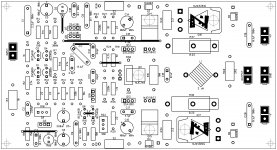
I've done some chassis drawings to fit Modular NS series boards and all associated parts into a 300mm deep 4U chassis from the DIYAudio store. I don't have a chassis in front of me to physically measure so I am relying in published dimensions for this so use these at your own risk and verify dimensions first if possible. If anyone can provide accurate physical dimensions of these chassis it would be much appreciated.
The output boards are 300mm deeps so this requires trimming 2.5mm off the front edge of the output boards (empty board space) and re-drilling the front board mounting holes to allow enough space to get the input connector depth correct. There are drawings to construct supply / control board mounts and a mount bracket to vertically mount a pair of transformers.
The drill templates can be adapted to just about any chassis. They are drawn to fit legal size paper. Distance from the rear edge and the top edge are critical so line those two edges up with the heat sink.
Attachments
Andrew,
I bought 5 UPC1237 speaker protection IC's from Ebay. They were very cheap so I thought so what, get them. In the end only two of them were close to specs. So I suspect that they were rejects.There are not a lot of those circuits that could be re branded. They worked, but not as they were meant to be. Eg, on a fault condition they take a second or two to switch, not immediately. But luckily two out of the five are ok.
I bought 5 UPC1237 speaker protection IC's from Ebay. They were very cheap so I thought so what, get them.
In the end only two of them were close to specs. So I suspect that they were rejects.There are not a lot of those circuits that could be re branded. They worked, but not as they were meant to be. Eg, on a fault condition they take a second or two to switch, not immediately. But luckily two out of the five are ok.Andrew,
I bought 5 UPC1237 speaker protection IC's from Ebay. They were very cheap so I thought so what, get them.
In a situation like that I would be concerned about the long term reliability of the whole batch and discard them all.
Parallel LT BJT OP
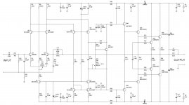
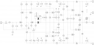
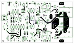
Hi Valery and Jeff and Fellas here.
I am a bit in twice about Parallel LT with Bias spreader as shown in Schema from Juli # 821 and later presented Board in August.
Bei observing every trace and part placement i found a added 1Mohm Resistor
and the 10 Ohm differs also in placement to Schema.
So i am wondering wich one is right now?
Is it a real tested board?
It seems no one was interested to work on parallel Luxman clone Topologie,
So i show here what i have done at the moment.
Attachments
Hi Valery and Jeff and Fellas here.
I am a bit in twice about Parallel LT with Bias spreader as shown in Schema from Juli # 821 and later presented Board in August.
Bei observing every trace and part placement i found a added 1Mohm Resistor
and the 10 Ohm differs also in placement to Schema.
So i am wondering wich one is right now?
Is it a real tested board?
It seems no one was interested to work on parallel Luxman clone Topologie,
So i show here what i have done at the moment.
Hi Bangla,
See the latest update of the schematic.
R19 (1M) just allows more precise trimming of the bias adjustment threshold - reducing this value you can move the threshold to the lower bias values if required.
Cheers,
Valery
Attachments
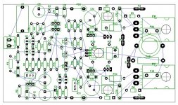
Parallel LT Beast
Thank you Valery.
Very, very kind help. That brings me a step forward.
Now i can overview where my brain stopped working.
So i have added updated parts in schema now.
Next problem (for me) now: if i renew design by components- all my pattern
work is lost- in different times i don't find out how to do.
Only way maybe a second copy?
My last tiny progress.
Regards.
Attachments
You need to change your patterns in the schematic, not the layout. That way changes are will remain. In the schematic right click on the part you want to alter and select replace part or go into the parts properties and select Attached Pattern and change it there. As long as the RefDes and the net names haven't changed everything will remain when you renew the layout.
- Home
- Amplifiers
- Solid State
- Revisiting some "old" ideas from 1970's - IPS, OPS