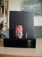
Prototypes
The bord is going to be doublesided, and if I can afford it I'll have them made with plated thou holes.
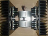
Yes the heatsink is too small, but since it's a prototype i did nor wnat to drill any holes in the heatsinks I'lll use for the final amp. (They are too expensive those things)
\Jens
The bord is going to be doublesided, and if I can afford it I'll have them made with plated thou holes.
Yes the heatsink is too small, but since it's a prototype i did nor wnat to drill any holes in the heatsinks I'lll use for the final amp. (They are too expensive those things)
\Jens
Attachments
Prototypes done
Hi again,
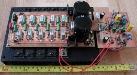
I got the small signal PCB done today, and good news it's alive !!
Notice the read wires going in the air it's from the 4 thermal compensating diodes, here mounted on the back of one of the output transistors (to get a quicker detection since my heatsinks are 6,8 kg each it will take so long for the thing to heat up that it might cause damage to the transistors)
The small board connecting the two parts will in the final version have a groundplane on one side.
Consept:
General purpuse output board
Whatever input board you want to try out (other than the Leach)
any idears are welcome
\Jens
Hi again,
I got the small signal PCB done today, and good news it's alive !!
Notice the read wires going in the air it's from the 4 thermal compensating diodes, here mounted on the back of one of the output transistors (to get a quicker detection since my heatsinks are 6,8 kg each it will take so long for the thing to heat up that it might cause damage to the transistors)
The small board connecting the two parts will in the final version have a groundplane on one side.
Consept:
General purpuse output board
Whatever input board you want to try out (other than the Leach)
any idears are welcome
\Jens
Attachments
PCB design
Jens,
First of all let me state that what I'm going to ask is a query, not a critic.
Why do you think it's worth it using double sided pcbs on a power amp?
I think I have seen very few using a double sided pcb, and when I did it was mostly for size reasons. That is for making it smaller.
Making a double sided pcb is difficult for DIY, even more when when metal-through-holed. What should justify it?
People like Nelson Pass might have something to say on this matter. Are you there?
In any case I do approve the design you did for the output stage, filling as much copper as possible. Making thick tracks is something we can do if we design our own.
Carlos
PCB Design
Reasons for double sided PCB's
1) When making a pcb, people often use 35µm cubber, that's not enough, therefor I made the PCB with wide tracks for the rails and output, and on both sides.
2) The design is made in such a way that it does not need plated throu holes (but I hoping to save enough meney to get real PCB's made)
3) The price for the prototype PCB's is less than US $10, and the PCB's were made using "films" printed on my printer on some semi transparent paper.
4) The PCB can be made smaller (and tracks shorter) and ground plane gives better EMC.
I could make singel sided PCB's but the generally get bigger, and there are more problems getting the right sort of ground implemetation on the board.
If there is general interrest I will put some effort in getting the PCB's made so people can by them.
I also plan a smaller version with 4 output transistors.
thanks for any comments
\Jens
Some numbers and components
Well, i fired it up using:
Rails = 55 V That's what im ending up using, since I have two 800 VA transformers.
BC546B/556B in the input stage (If the originals are to be used (MPSA06/56) they need to be turned 180 degrees form the 546/56 models)
VAS an predrivers are BD139/40 (Will be changed into MJE340/50) when the arrive
Drivers are MEJ15032/33
Outputs are MJL3281A/1302A
Working current in each transistor.
All resistors are 5 % ones exceps the 11kohm they are 1% taken without testing their value.
DC ofset -20 mV
Since school has changed into win2k our test equepment is out of order, so I'll be back with THD measurements and freq response.
\Jens
PCB design
Jens,
My experience is not large, but I did design and/or built maybe 40 or 50 projects. Most single sided, a very few single sided. Most DIY, a few for commercial products.
Some of the fist ones were done using transfers for the prototypes; on others I implemented a way of my own using paper tape instead of transfers. That was done in order to make wider tracks.
Lately I used a place here that can get me decent prototypes.
So I partly agree with your first reason in widening tracks. I also believe in pads being square, as they make getting closer with the tracks or wider. But I think ALL tracks should be wider, not just power or ground tracks.
Now if you tell me you will use the components side for power and ground tracks mostly that is certainly a good reason for going double-sided. You shouldn't duplicate the same connection on the upper and lower sides though.
Designing double-sided to avoid metal-through is certainly possible, but it gets tricky when you use ICs or very small pcbs, where parts are very close together. Assembling your own double-sided pcbs is quite a problem though, and it's better done by a pro place.
The price you mention for prototype pcbs is for what size?
What film and printer did you use for the final art? The only print I have seen that was dark enough was on 3M film and printed on an Epson. My HP 640 doesn't seem to print thick enough.
The best benefit from double sided pcbs is they simplify the laying of tracks, making tracks shorter. Ground planes seem to be effective at RF only, so they may not be reason enough to go double-sided.
Single sided boards are probably larger most of the times, or will need a few jumpers, but even pro designs use them.
Implementing a star ground is certainly a must. In my case I think even power lines should be star designed.
It would be great if we could get to a simple, working way that we could all use to design and build our pcb projects. That would allow designing for the specific parts size we are going to use.
Last but not least: your pcbs look great!
What did you use to protect the copper? Some specific lacquer or varnish?
Carlos
PCB layout
The prototypes are about
Outputboard
10 * 20 [cm]
Small signal Board
10 * 9 [cm]
Double sided non plated.
I use a HP Laserjet 6L (Older model) and the "film" is som semi transparent paper from the schools bookshop (I'll se if I can find the brand it's about 1/4 US$ per sheet in size A4)
There is groundplane an rails on both sides of the PCB.
Ground plane means that I can make my starpoint in the PSU. (Not designed yet)
I use a program called Eagel for schmatics and PCB, It's really two programs running together, and thereby making sure that schmatics and PCB is correct compared to eachother.
I used a clear coating that you can solder on. (again I'll find the brand, it's from my school's workshop)
Carlmart why do you want all tracks wider ? I mean the input stage draws about 3 mA, no reason for a 250 mill track for that I think.
Thanks for any reply
\Jens
Tracks
Jens,
>why do you want all tracks wider ? I mean the input stage draws about 3 mA, no reason for a 250 mill track for that I think.
Many reasons, mostly dealing with assembly/disassembly process. Right now I'm modifiying an ART DI/O DAC where pads and tracks are small and thin, some of them peeling off quite easily.
Using different part types, including SMDs, becomes much easier. From what I could find out, having large copper surfaces is only bad for production soldering assembly, but it can be something we DIYers can take advantage of.
Even if currents are low, as you rightly mention, I guess several areas might benefit from wider tracks.
Please do comment what would you have against them.
Carlos
Tracks
Wider tracks take up more space, that's the only thing i have agains them.
The width of my small signal tracks is 40 mill = 1 mm, that I considered a wide track. When dealing with SMD technology and low currents it's not uncommon to use tracks that are 1/10 mm.
If you worry about the ohmic resistrence in the track with small currents, don't !!. What's important is the inductance of the track.
A rule for designing tracks states that a wire has about 1.5 nH/mm, and something similar can be used for tracks on a PCB.
I am using bigger solderpads where there is room for it, but how much cubber do you want for a 0.8 mm hole ? I'm using pads that are about 2 mm wide for 0.8 mm holes.
When the components are bigger or havier, the pads are chosen to be as big as possible, but not so big that heating them up when soldering may cause damage to components. Generally you don't want to apply heat for more than 2 - 3 seconds when soldering on semiconductors (And even less with SMD's !!)
\Jens
Progress
Hi
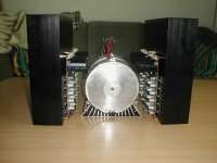
Today the first two of four outputboards got mounted on the heatsink, they both worked")
I'm working on the final layout of the small signal PCB's, they will problably be ready in two weeks or so.
One question though:
The outputinduction, how big does it need to be ? I tried to freq. sweep the amps, and the response seem to flat until about 25 khz. I'd like it to go a bit higher, say about 50 khz or so.
Thanks for any reply
\Jens
Hi
Today the first two of four outputboards got mounted on the heatsink, they both worked
I'm working on the final layout of the small signal PCB's, they will problably be ready in two weeks or so.
One question though:
The outputinduction, how big does it need to be ? I tried to freq. sweep the amps, and the response seem to flat until about 25 khz. I'd like it to go a bit higher, say about 50 khz or so.
Thanks for any reply
\Jens
My project
Hi
Well I don't know the brand of the heatsinks, I just ordered them from aavids danich destrubitor, I only know that it's a standard profile made in custom lenghts for me
Yes the amp will have four channels, I took the advice from a couble of people in the forum.
I mean to use it for Bi - amping, and for bridging when it's party time.
\Jens
Small PCB
Hi Brian
Great to hear form you, hope all is well with your new home
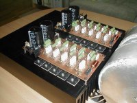
I have not decided yet where to mount the small PCB's, but most likely it will be on the heatsinks in the top end. Like the pic of my prototype PCB.
I need to find out about the slow start circuit though.
I would like to know what causes the large inrush current.
Is it:
a) The transformer
b) The large caps
c) a + b
What would be the best means to ensure that the current is controlled ?
Thanks for any reply
\Jens
Hi Brian
Great to hear form you, hope all is well with your new home
I have not decided yet where to mount the small PCB's, but most likely it will be on the heatsinks in the top end. Like the pic of my prototype PCB.
I need to find out about the slow start circuit though.
I would like to know what causes the large inrush current.
Is it:
a) The transformer
b) The large caps
c) a + b
What would be the best means to ensure that the current is controlled ?
Thanks for any reply
\Jens
- Status
- This old topic is closed. If you want to reopen this topic, contact a moderator using the "Report Post" button.
- Home
- Amplifiers
- Solid State
- redesign of leach amp pcb for integrated TO-247 output devices