Hi,
I have a few doubt about the darlington pair characteristic. After reading all the sources, i know that darlington pair has a higher current gain and a low input impedance. Then i start to prove it through experiments.
Figure1 is the common collector by using one transistor. and Figure2 is common collector using a darlington pair. Both has the same resistors value.
Figure1
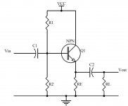
Figure2
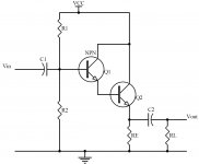
after calculation i found that, the Figure2 design just increase the input impedance by 4k ohm. And Ic for Figure1 is ~4.7mA while Ic for Figure2 is ~4.37mA. So what i curious about is isnt it Figure2 should have a more higher current compare to Figure1? If not what is the purpose i use the darlington pair since i get almost the same Ic by using the Figure1 design.
This is the question i cant figure out.
Hope someone can help me on this.
thank you.
I have a few doubt about the darlington pair characteristic. After reading all the sources, i know that darlington pair has a higher current gain and a low input impedance. Then i start to prove it through experiments.
Figure1 is the common collector by using one transistor. and Figure2 is common collector using a darlington pair. Both has the same resistors value.
Figure1

Figure2

after calculation i found that, the Figure2 design just increase the input impedance by 4k ohm. And Ic for Figure1 is ~4.7mA while Ic for Figure2 is ~4.37mA. So what i curious about is isnt it Figure2 should have a more higher current compare to Figure1? If not what is the purpose i use the darlington pair since i get almost the same Ic by using the Figure1 design.
This is the question i cant figure out.
Hope someone can help me on this.
thank you.
Your example is setting a fixed voltage on the base of the transistors via R1 and R2.
So the darlington will actually give a lower voltage across Re and thus an apparently lower Ic. It's lower because there are two base emitter junctions in the darlington configuration.
What the darlington does do is give a huge current gain. Remember bjt transistors are CURRENT driven, not voltage driven.
So if you remove R1 and R2 and replace just R1 with say 1meg ohm the first circuit will not develop much voltage across Re. The darlington will... the current gain is much higher.
hi Mooly, thanks for the reply.
I can see that if i scale R1 and R2 upward (R1x10) and (R2x10) then the input impedance will become higher and Vout has a very very little increase which is almost the same as the Vin. Power delivered to the load still the same.
Am i correct?
thank you.
I can see that if i scale R1 and R2 upward (R1x10) and (R2x10) then the input impedance will become higher and Vout has a very very little increase which is almost the same as the Vin. Power delivered to the load still the same.
Am i correct?
thank you.
Imagine Re to be a bulb... say a car headlight that draws 5 amps or so and you want to switch it on or off with a small control current perhaps from a microprocessor that can only supply a very low current. This is where the darlington could be used as it would operate with only a few milliamps of base current, the single transistor would need hundreds of milliamps of base current.
That's essentially correct yes.
The darlington gives an effective current gain of the combined hfe's of the two transistors.
But Mooly,
Although i increase the R1 and R2 value but it still wont affect my Vb value and so the Ie. And Ie = Ic . Am i correct? So i still can get the same Ic by using the Figure1 design right? then why i want to choose the darlington design?
thank you
You have to start thinking in terms of current as well as voltage.
Ve = Vb less 0.7 volts (for a single silicon transistor).
Ie = Ib + Ic.
Vb is affected if there is not enough current available to supply the bias requirement of the transistor. The transistor pulls current from R1 and R2 and lowers the voltage (Vb).
If the transistor is high gain (a darlington) the current it draws from R1/2 is less.
Not easy to explain in a few words
or maybe i should say if i want to prove that a darlington pair has a higher current than a basic common collector amplifier. Then i use the same R1 , R2 , Re and RL value for both figure1 and figure2. I still get almost the same Ie and Ic. Just that figure2 has higher impedance. This is the main point i cant understand, why darlington pair has higher current and my experiment couldnt prove it. And this makes me hard to understand and confuse.haha...
thank you
thank you
Because it has higher current gain! You need to remember that current gain is a ratio, not an absolute value. In most cases the output current of a Darlington is set by the circuit, and may be exactly the same as a single BJT used in the same circuit. Then the higher current gain of the Darlington manifests itself not as increased output current but as decreased input current. I think your problem is that you are thinking of gain as necessarily meaning a bigger output from a given input, when it can also mean a smaller input for a given output.
But Mooly,
Although i increase the R1 and R2 value but it still wont affect my Vb value and so the Ie. And Ie = Ic . Am i correct? So i still can get the same Ic by using the Figure1 design right? then why i want to choose the darlington design?
thank you
Lets put some numbers in to try and show what happens in basic terms... trying to make this simple without going into the finer details.
Using your first diagram and looking at DC conditions.
Supply voltage = 10volts
R1=10K (10000 ohm)
R2=10K
Re = 100 ohm (low but valid)
The transistor is a high power type of hfe 15
The maximum base current available is 10 volts divided by R1. You can not get more current than that to flow in R1 and that works out to 1 milliamp.
With a current gain of 15 that means that if all that 1 milliamp flowed into the base, only 15millamps approx would flow in the collector-emitter path. That 15 milliamps would develop only 1.5 volts across Re when you might have expected it to be nearer 5 volts.
Now look at the darlington. We add a transistor in front of the first and lets say that this one has a current gain of 100 as we might choose a medium power type of device for this. The hfe of the darlington is now 100*15 which is 1500.
That means that our 1 milliamp could in theory allow 1500ma (1.5 amps) to flow in the collector-emitter path. We now have plenty of current available and this current will develop a voltage across Re (the 100 ohm). The voltage across Re will be close to the voltage on the first base of the darlington (now approx 5 volts) less two base/emitter junctions each dropping 0.7 volts. So the voltage across Re would be 5- 0.7 -0.7 which is 3.6 volts.
Because of this B-E volt drop we would have to alter the value of R1 or R2 slightly to make the base voltage equal 5 plus 0.7 + 0.7 which is 6.4 volts in order to get 5 volts at the emmitter.
We can work back and say that 3.6 volts across 100 ohm produces a current flow in Re of 3.6/100 which is 36 milliamps.
We know the gain of the darlington is 1500 so the base current is 36ma divided by 1500, which is 0.036/1500, which is 0.000024 amps.
So only 0.000024amps is needed from the bias network.
And going back to the first example of a single transistor.
We want the voltage across Re to be approximately 5 volts. Our transistor has a gain of only 15. That means that 5 volts across 100 ohm (Re) means we need 50 millamps flowing. With a gain of 15 that means at least 50 divided by 15 which is 3.33 milliamps is needed.
So our resistors of R1 and R2 must be decreased dramatically to make that sort of current available to the base.
Not only that, when you are determining a bias network you have to take into account the "load" that the base will apply (the current drawn) and scale the network such that it is imune to that load. If it were marginal then the normal spread of transistor gains would mean every transistor gave a different voltage across Re. We overcome that by making the current in the bias network orders of magnitude greater than that needed by the transistor base current.
Does that make sense...
So i still can get the same Ic by using the Figure1 design right? then why i want to choose the darlington design?
Because then you can use higher values of R1, R2 without the current through the transistor base affecting the bias point.
It's usual to choose R1, R2 so that the current through them to ground is 10 times the (quiescent) current into the base. This makes the voltage divider 'stiff', and the bias point predictable and stable.
The voltage at the emitter in this case is ~ (R2/(R1+R2)) - 0.6V. If R1=R2, this is approximately halfway between Vcc and Ground, but if the current into the base is large compared to the current through R1, R2 then this is not true, the voltage sags toward Ground and the possible voltage swing at the emitter is reduced.
The input impedance of the stage is dominated by R1 in parallel with R2. If the current into the base is small, R1 and R2 can be large, and the input impedance will be large.
Hi Mooly,
Your explanations really make sense.haha.. all right. let me figure out y'all explanations first.thank you. will update to u all soon.
thank you.
Do you have some real transistors and a PSU to play around with because that is the only way you will learn really ?
hi Mooly,
yes.I'm have construct the Fig1 which is a CC amplifier circuit. R1=2.2k R2=2.7K RE=330 and RL=330.
Then i do some calculations and measurements on the circuit.
One thing i found out is that if i increase the amplitude of the input signal to more than 200mVpp, then the calculation is somehow different with the measurement value for the Vin part.
Below is my calculations:
Zin = 1.16k ohm
Vin = [Zin / (Rs + Zin)] * Vgenerator
= [1.16k / (350 + 1.16k )]* 0.071Vrms
= 0.055V
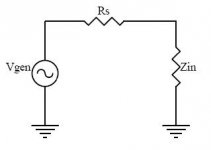
Then, Vout = Vin for CC. So i assume Vout to be 0.055Vrms.
But from my measurement i get 0.068Vrms which is much more higher than my calculation. Then i decrease my Vgen to 0.037Vrms. After calculation i get 0.028Vrms and i get 0.032Vrms for my measurement value which is much more nearer for both calculation and measurement.
Any idea?
thank you
yes.I'm have construct the Fig1 which is a CC amplifier circuit. R1=2.2k R2=2.7K RE=330 and RL=330.
Then i do some calculations and measurements on the circuit.
One thing i found out is that if i increase the amplitude of the input signal to more than 200mVpp, then the calculation is somehow different with the measurement value for the Vin part.
Below is my calculations:
Zin = 1.16k ohm
Vin = [Zin / (Rs + Zin)] * Vgenerator
= [1.16k / (350 + 1.16k )]* 0.071Vrms
= 0.055V

Then, Vout = Vin for CC. So i assume Vout to be 0.055Vrms.
But from my measurement i get 0.068Vrms which is much more higher than my calculation. Then i decrease my Vgen to 0.037Vrms. After calculation i get 0.028Vrms and i get 0.032Vrms for my measurement value which is much more nearer for both calculation and measurement.
Any idea?
thank you
Here's what I did 
My generator has a constant 50 ohm output impedance so I added a 300 ohm series resistor to bring it up to 350 ohms (your Rs).
I built your circuit using a BC107B running on 12 volts.
Input freq 1khz.
Coupling caps 220uF
Generator set to 71mv rms (checked using meter and scope)
Connecting the generator caused the signal at the generator output to drop to 54.6mv.
[71mv less 54.6mv is 16.4mv which is the voltage "lost" across the generator output impedance. That equates to 4.685e-5 amps. The input impedance Zin is 54.6mv/4.685e-5which is 1165 ohms.
The signal measured at across Re was 54.0 mv which tallies with the "less than gain of 1" for a CC or emitter follower. The output impedance is low and pretty independant of Re. It's actually a function of the "transimpedance" of the transistor.
I repeated the test with a TIP41C which reduced Vin from 71mv to 54.1mv and gave an input impedance of 1120 ohms.
Why your descrepancies... how are you measuring the voltage ? DVM's may not be very accurate at low level and are certainly not if the frequency is outside their working spec.
Hum and noise can affect readings too.
- Status
- This old topic is closed. If you want to reopen this topic, contact a moderator using the "Report Post" button.
- Home
- General Interest
- Everything Else
- Question regarding darlington pair