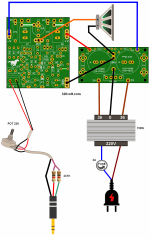
Hello, I designed a new PCB. It works very well


Source: http://www.videorockola.com/proyect...ificador-monofonico-de-100-watts-version-2-0/
Source: http://www.videorockola.com/proyect...ificador-monofonico-de-100-watts-version-2-0/
Attachments
Last edited:

It is similar topology to Hitachi circuit
and very simplified version of early op amp.
On a positive note it is favorite topology of mine
and also love Quasi Outputs as well.
I will assume Q1 , Q2 current levels
are way to low to help stabilize the amplifier.
And Q3, 4 and 5 currents are also way to
low. Simple balanced Vas can just be all matching
devices. Tip42 or assume C suffix or TIP42C
for 100 volt devices. Poor choice
and would need higher current to be linear.
For Q3/4
Current is likely no higher than 2ma
R8 needs parallel capacitor to stabilize the circuit.
Around 6.8 to 10n.
Which is why I assume C6 / C7 1n !! were added to stabilize
the amplifier. If current levels and 2nd gain stage
were correct such massive compensation would not be
needed.
The slew rate above 10k frequency signals
would be rather horrible.
Very great idea, lovely topology
and seemingly very compact nice PCB.
Current levels, Transistor choices and stability compensation
not well done.
Transistor output bias is kept very low class B
This can help Current sharing with quasi output with no
Baxandall Diode. Otherwise with higher bias, diodes for bias
dont bother me as much as others, but need to be placed on main
heatsink for thermal tracking. This amp has high emitter values
and very low bias. So likely not much of a issue.
But for A/B operation thermal track the diodes or use VBE multiplier.
And Quasi output needs baxandall diode.
Circuit will be more linear and without it and normal A/B bias
AC current will all go mostly to one NPN output.
Looking at input resistors/gain resistors and very low current
for all gain stages I assume high DC offset on output and noted
stabilization issues.
Tip 42 of course will get bashed is horrible device.
But if used on 50 volt rails/ 100 volt supply. Should note C suffix
devices which are 100 volt.
Last edited:
@WhiteDragon can you draw a better schematic with appropriate components? It would be great.
Regards
Regards
@NanoFarad
Yes I could.
Would it be for similar rail voltages / power levels of 50 volts.
And also this is BJT output section, OP shows Quasi Complementary output topology.
Would you like Quasi output for similar Balanced Vas frontend / Hitachi
Or should I just make output section Complementary.
Im a fan either way, and would just use higher speed devices and Baxandall diode
for proper Quasi Output.
Maybe could make separate thread, this is amplifier I desire and would hope to
bring in somebody to do actual board.
I can and have made some changes
Stability is tradeoff as always with THD numbers / slew rate etc etc.
I lowered differential degen R20, R15 to 180, was high at 470 before to get such High Ft output section
to be stable. I was trying to keep slew rate high but raised C5 to 22p for not much difference and got THD1
distortion rating. To be where I would expect it to be with this topology. Around .001 to .008 typical
Also had to get current of T7 and T8 to match, otherwise typical Quasi behavior
and you can have stability issue at high frequency, or AC current sharing of output
transistor can be uneven. And with Quasi even if DC offset is pretty as can be.
AC current sharing is not equal in output section, Its just how good are you, and how close
you can get. Any ways by changing R3 and R26 and R17. To different values to balance
current of EF and CFP sections. And this also resulted in more stable high frequency.
Here is new schematic with DC current values shown
And yes Differential is using only 1ma NOT 2ma like normally seen.
And yes it has Degen like not normally seen. Because it is 35 Mhz output
devices and it is stable amplifier.

THD1 (1 kHz) with 1 volt RMS input .004%
With good Quasi , yes strong 2nd Harmonic profile


THD20 ( 20 kHz) with 1 volt RMS input .05%
Second Harmonic still high with typical higher 3rd harmonic at higher frequency


Square Wave at 22 kHz

Sine clipping behavior at 1 kHz

As you see lower Quasi rail clips well as expected with added
Baxandall Diode. Slight Rail stick on positive portion is not Output
Section. That is typical of Hitachi style balanced Vas.
If R7 10k is raised to 12k or 15k then rail stick is reduced/ removed.
But THD and Vas balance will be pure garbage.
No way to change and typical of simplified topology.
You would have to add mirror and current source.
Or about 4 to 6 more transistors. So = Ignore
AC transfer

Stability is tradeoff as always with THD numbers / slew rate etc etc.
I lowered differential degen R20, R15 to 180, was high at 470 before to get such High Ft output section
to be stable. I was trying to keep slew rate high but raised C5 to 22p for not much difference and got THD1
distortion rating. To be where I would expect it to be with this topology. Around .001 to .008 typical
Also had to get current of T7 and T8 to match, otherwise typical Quasi behavior
and you can have stability issue at high frequency, or AC current sharing of output
transistor can be uneven. And with Quasi even if DC offset is pretty as can be.
AC current sharing is not equal in output section, Its just how good are you, and how close
you can get. Any ways by changing R3 and R26 and R17. To different values to balance
current of EF and CFP sections. And this also resulted in more stable high frequency.
Here is new schematic with DC current values shown
And yes Differential is using only 1ma NOT 2ma like normally seen.
And yes it has Degen like not normally seen. Because it is 35 Mhz output
devices and it is stable amplifier.
THD1 (1 kHz) with 1 volt RMS input .004%
With good Quasi , yes strong 2nd Harmonic profile
THD20 ( 20 kHz) with 1 volt RMS input .05%
Second Harmonic still high with typical higher 3rd harmonic at higher frequency
Square Wave at 22 kHz
Sine clipping behavior at 1 kHz
As you see lower Quasi rail clips well as expected with added
Baxandall Diode. Slight Rail stick on positive portion is not Output
Section. That is typical of Hitachi style balanced Vas.
If R7 10k is raised to 12k or 15k then rail stick is reduced/ removed.
But THD and Vas balance will be pure garbage.
No way to change and typical of simplified topology.
You would have to add mirror and current source.
Or about 4 to 6 more transistors. So = Ignore
AC transfer
Last edited:
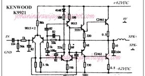
Greetings, I would like Mr. WhiteDragon if I could simulate something similar with a mosfet N output but keeping it very simple like the original Hitachi and in that same voltage range between 35v and 50v, as simple as this Kenwood
Attachments
- Home
- Amplifiers
- Solid State
- Quasi Complementary Amplifier New PCB