I attached a schematic of a generic PSU that I would like to order PCBs for - I did this one in EasyEDA since it seemed easy enough to do the schematic and order the boards. I have never flipped a schematic to PCB and it seems to not be converting the way that I would like. Please disregard the 1k value on the bleeder resistors as the value would change but I want to make sure that I have enough room to use any power resistor needed - same applies to the 10kuf caps; I used that value to make sure that I have a large enough pad to use up to a 10kuf cap in that space. I can do it in another program and import the files if doing it in Kicad is easier to make a PCB file there then the easyeda software. I was hoping someone can assist me with the following questions so that I can finish and order the PCBs and add a few things to it after clarification:
1) Is there a figure/component I can use to let the software know that I would like to use a fast-on QD at certain points?
2) I would like to add DC1 and DC2 so that I am able to have 2 different voltages being rectified and available after the capacitors...I am sure a multi layer board will be needed but how am I able to show this in the schematic?
3) I would like to add a terminal for use with center tap hot and 0v connections in addition to the v-0-v configuration. To do this do I just add a common connection for what becomes the + and - before the rectifying diodes?
4) I would like to add an AC AUX terminal to the board...I suppose I just make another trace to fast ons coming from the AC mains connection to do this?
5) Is there anything else you think I should add or change on this?
Thank you in advance for your help - I need to order at least 10 of these to start off and if you would like a board in return for your assistance/knowledge/help, please let me know and I would be glad to order extras and ship it out to you.
Best regards,
Jared
Attachments
Yes I know center tap goes to zero but would like to add a fast on for transformers wired in series or parallel. Basically so center tap goes to 0 and the 2 ACs are combined. Hope I am explaining it correctly. I prefer the PCB to hold the diodes and caps tight as well as having multiple voltages being rectified. How am I able to add a second voltage path to the schematic so that the PCB design is accurate?You don't really need a PCB for such a simple supply. 0V goes to centre tap on the transformer
would like to add a fast on for transformers wired in series or parallel. Basically so center tap goes to 0 and the 2 ACs are combined. Hope I am explaining it correctly. having multiple voltages being rectified. How am I able to add a second voltage path to the schematic so that the PCB design is accurate?
Sorry, a lot of this isn't clear to me, please draw a diagram of what you mean. Also, what do you mean "fast on"?
Sorry, a lot of this isn't clear to me, please draw a diagram of what you mean. Also, what do you mean "fast on"?
I don't know how to draw a schematic of what I want to do. I would like 2 electrical paths so that 2 different voltages are using the rectification and smoothing. I would also like terminals for both a v-0-v and "hot" 0v connection for the AC. The "fast on" connections are the quick disconnect spades that mount to PCBs.
Thanks,
Jared
Ah, I know what you mean by fast on, didn't realise you ment the connectors. Please don't take this the wrong way, but if you don't know how to draw a schematic you shouldn't proceed until you do. Read all about power supplies. The Elliott Sound Products site is a very good place to start
Ah, I know what you mean by fast on, didn't realise you ment the connectors. Please don't take this the wrong way, but if you don't know how to draw a schematic you shouldn't proceed until you do. Read all about power supplies. The Elliott Sound Products site is a very good place to start
No offense taken. I do know how to do a schematic and did this one. I don't know how to express another path for the secondary voltage, just an educated guess. I know I would obviously need to show the additional lines in and out of the rectification diodes but how do you express it in a schematic so when the program does PCB each voltage rail is on a separate layer? It seems that just labeling it wouldn't do anything for PCB routing and the rails would end up merging rather then being separate individual voltages. I also can't figure out how to place the connections- the schematic software has them however when I try and convert to PCB it says the connections are errors so I have to remove them. So I guess while I can do a schematic of what I want, flipping it to a PCB is where I am having trouble. I can update one now showing the extra rail and terminal connections if you would like - perhaps you can tell me how to change it so the PCB will route correctly?
To start designing this PCB is pretty simple, draw the physical components on a piece of paper in a way that you would like it to look. In other words the large capacitors will be circles each with two connections, a plus and a minus....
Once you have draw the design pictorially, seen from the top, looking down onto the fictitious board, connect the connection points (called nodes). The result is a PCB layout, in other words where the connection lines are is copper and where there is no line are the spaces between the copper tracks.
In this case it need not be multi-layer all the copper tracks are on bottom side of the pcb and the top is where the components are placed through holes drilled in your board and soldered to the pads.
There are programs (the one you used) that will automatically place copper between the components connections using what is referred to as a net-list. A net list in effect is the component such as C1 and the positive connection would be say, 1 while the negative connection is 2. The node is defined as C1,1 (the positive connection of capacitor 1) and the net will be the end point of the connection, say Resistor R1,1 (1st connection of R1).
A net list is generated from your schematic connections you have drawn and contains all the points connecting the various nodes in the schematic.
What one has to specify is how wide your track must be and the sizes of the solder pads and also the minimum gap between the various tracks. In effect this was a very simplistic explanation of designing a PCB.
One question was that you want to use quick or "spade" connectors. As you have done with the capacitors and other components you have to find the connector of choice and give it a name, say CON. This connector is then assigned the part number that you would refer to when you purchase it. You will have to find or create a physical PCB and schematic diagram for CON or you may use something in existence in the schematic design package say a small circle.
In order to finish your schematic diagram from the first post you have to get a connector and place one everywhere you want to make a connection. At each of the inputs to the left of the fuses, and each of the outputs to the right of the fuses, then one on each of the ground connections.
It would be smart if the three inputs from the transformer are closely spaced and on one side of the board, while the pos, neg and ground for the output could be on the opposite of the board.
I hope this long-winded explanation help.
If it was too simplistic please forgive me.
Last edited:
Your question in post 7 is simply answered in that you can have as many "wires" coming of a node as you would like. However I do not see the nodes between the diodes and assume that you did not place a wire connection between them. The node of course is the round dot.
If you wanted to make another connection to a point on the same net (wire between two points) you can do this and the program would ad another node (red dot) and the net wire connection will then have three nodes.
In the olden days we did wire crossing each other with a little bridge, nowadays two wires crossing that don't show the red dot is exactly that, with no node showing it is a crossing.
A crash course in PCB design is not easy, it is really something to play with, and one PCB design package could be totally different from another. The only really common thing is the output plot which is a gerber plot and very much like the old Hewlett Packard plotters worked using pen up and pen down, left right, etc.... That is what they use to generate the high resolution PCB layout.
Ok, gotcha, I'm an ol' skool kinda ol' guy, I don't use programs for this stuff. I'm sure someone will be along to help you with this modern, newfangled computer lingo now they realise it's beyond my ken. Soz.
To be honest I could have done it free hand over and over by now. I do need to learn the software tho and doing it for something simple first seems like a good idea.
You just keep on adding as many faston pins as you like in the sch and they will be reflected on the layout.I attached a schematic of a generic PSU that I would like to order PCBs for - I did this one in EasyEDA since it seemed easy enough to do the schematic and order the boards. I have never flipped a schematic to PCB and it seems to not be converting the way that I would like. Please disregard the 1k value on the bleeder resistors as the value would change but I want to make sure that I have enough room to use any power resistor needed - same applies to the 10kuf caps; I used that value to make sure that I have a large enough pad to use up to a 10kuf cap in that space. I can do it in another program and import the files if doing it in Kicad is easier to make a PCB file there then the easyeda software. I was hoping someone can assist me with the following questions so that I can finish and order the PCBs and add a few things to it after clarification:
1) Is there a figure/component I can use to let the software know that I would like to use a fast-on QD at certain points?
2) I would like to add DC1 and DC2 so that I am able to have 2 different voltages being rectified and available after the capacitors...I am sure a multi layer board will be needed but how am I able to show this in the schematic?
3) I would like to add a terminal for use with center tap hot and 0v connections in addition to the v-0-v configuration. To do this do I just add a common connection for what becomes the + and - before the rectifying diodes?
4) I would like to add an AC AUX terminal to the board...I suppose I just make another trace to fast ons coming from the AC mains connection to do this?
5) Is there anything else you think I should add or change on this?
Thank you in advance for your help - I need to order at least 10 of these to start off and if you would like a board in return for your assistance/knowledge/help, please let me know and I would be glad to order extras and ship it out to you.
Best regards,
Jared
I didn't understand the AC aux requirement also the dc1 dc2 requirement.
To start designing this PCB is pretty simple, draw the physical components on a piece of paper in a way that you would like it to look. In other words the large capacitors will be circles each with two connections, a plus and a minus....
Once you have draw the design pictorially, seen from the top, looking down onto the fictitious board, connect the connection points (called nodes). The result is a PCB layout, in other words where the connection lines are is copper and where there is no line are the spaces between the copper tracks.
In this case it need not be multi-layer all the copper tracks are on bottom side of the pcb and the top is where the components are placed through holes drilled in your board and soldered to the pads.
There are programs (the one you used) that will automatically place copper between the components connections using what is referred to as a net-list. A net list in effect is the component such as C1 and the positive connection would be say, 1 while the negative connection is 2. The node is defined as C1,1 (the positive connection of capacitor 1) and the net will be the end point of the connection, say Resistor R1,1 (1st connection of R1).
A net list is generated from your schematic connections you have drawn and contains all the points connecting the various nodes in the schematic.
What one has to specify is how wide your track must be and the sizes of the solder pads and also the minimum gap between the various tracks. In effect this was a very simplistic explanation of designing a PCB.
One question was that you want to use quick or "spade" connectors. As you have done with the capacitors and other components you have to find the connector of choice and give it a name, say CON. This connector is then assigned the part number that you would refer to when you purchase it. You will have to find or create a physical PCB and schematic diagram for CON or you may use something in existence in the schematic design package say a small circle.
In order to finish your schematic diagram from the first post you have to get a connector and place one everywhere you want to make a connection. At each of the inputs to the left of the fuses, and each of the outputs to the right of the fuses, then one on each of the ground connections.
It would be smart if the three inputs from the transformer are closely spaced and on one side of the board, while the pos, neg and ground for the output could be on the opposite of the board.
I hope this long-winded explanation help.
If it was too simplistic please forgive me.
Thank you. I would like to add a secondary tracing for an additional voltage. How do I do show it on a schematic where voltage 1 and 2 are not getting crossed on the output after the rectifier and caps? I would also like to add another spade input for the AC so that I can use a v-0-v toroid or I can use a multi voltage toroid with wires connected to give me the desired input voltage. I assume that part is easy however the multi voltage lines is what is giving me issues.
You just keep on adding as many faston pins as you like in the sch and they will be reflected on the layout.
I didn't understand the AC aux requirement also the dc1 dc2 requirement.
when i add the fast ons in schematic, I get an error and have to delete them only to add them to the pcb itself. AC AUX would just be another trace to an additional fast on to allow the AC input to go to another board that requires ac voltage - like a 12v transformer that is PCB mounted,etc. DC1 and DC2 is because I would like to use the same board to run 2 voltages thru the rectifier and caps - slightly higher rails for the IPS and VAS and slightly lower for the driver and output transistors.
Not sure if this is correct but it should give you a better idea of what I am trying to do. I would like 2 AC voltages being rectified and smoothed with the connectors prior and post fuses. Please let me know how to improve this.
Attachments
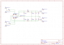
The way your sch is drawn is incorrect.Sorry, I didn't attach it correctly last time.
You can't use a single rectifier and one set of smoothening caps to run two different voltages simultaneously.
Draw two different circuits one below the other. the layout can have more than one circuit on a single board.
If there are common connections , e.g. ground, those can be denoted via symbols and labels.
The way your sch is drawn is incorrect.
You can't use a single rectifier and one set of smoothening caps to run two different voltages simultaneously.
Draw two different circuits one below the other. the layout can have more than one circuit on a single board.
If there are common connections , e.g. ground, those can be denoted via symbols and labels.
I figured this one was not accurate but gave it a shot. I am guessing the same schematic and PCB layout can be used on 2 different layers allowing both voltages to be isolated from each other. Holton Audio's PSU2 has 1 rectifier and 1 bank of caps however it is able to run 2 different voltages - I have a few of his PSUs however I would like a smaller board with bleeders on board to minimize the footprint so I know it can be done, just a matter of doing it correctly.
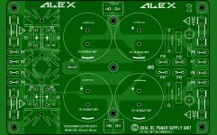
Hi Jared C79
I have layout this attached PCB , I hope it's what you need
Best regards,
Alex
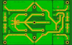
In your PCB design you force filter capacitors charging return currents to turn at 45 degree which makes it a perfect antenna for mains hum. You also force charging return and load return currents to go the same route which seems to be not so good to keep the GND potential stable. I would suggest to make one big copper pour for the GND without separate traces to all capacitors.
You also designed your PSU PCB for center tap transformer since you provide only one connector for the center tap. This makes it more difficult to use your PSU PCB with dual winding transformer. Instead of providing two connectors for the transformer upper/lower taps (which seems redundant) it would be better to allow for a second center tap connector (where two transformer secondaries can be connected in series).
You also seems to have redundant fuses on board. I think it is much safer to use fuses at the AC side than on each DC rail. This is because if one fuse on the AC side goes open you do not lose the DC rails, just the current capacity goes down and voltage sug increases which is typically not so bad. While in case of real failure both AC fuses will go off saving your circuit downstream. In contrast, if any of the DC rails go off due to single (DC side) fuse rupture your speakers face half (or full) rail DC voltage which they may not like.
To see a good layout just look at this one. prasi is currently running a second GB on it. Just navigate to the end of the thread linked above and sign up
Regards,
Oleg
- Status
- This old topic is closed. If you want to reopen this topic, contact a moderator using the "Report Post" button.