Just to contribute to the thread, here is a snapshot of Vgs of the lower side switch (between Vss and output), and the current in the sense resistor for the lower side switch when the amplifier is running idle. The polarity of this current is such that a negative voltage on the scope means that current flows from the load and into the lower voltage rail (Vss).
I cant really understand what is happening here, first the lower FET is active, but at the instant the switch opens there flows a current in the WRONG direction through the lower FET. Please help me understand this.
I cant really understand what is happening here, first the lower FET is active, but at the instant the switch opens there flows a current in the WRONG direction through the lower FET. Please help me understand this.
Attachments
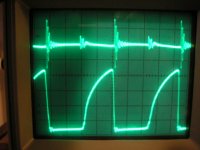
zilog said:Just to contribute to the thread, here is a snapshot of Vgs of the lower side switch (between Vss and output), and the current in the sense resistor for the lower side switch when the amplifier is running idle. The polarity of this current is such that a negative voltage on the scope means that current flows from the load and into the lower voltage rail (Vss).
I cant really understand what is happening here, first the lower FET is active, but at the instant the switch opens there flows a current in the WRONG direction through the lower FET. Please help me understand this.
Maybe I'm missing something, but I would expect the current to be a triangle wave centered about zero - just as shown in your photo (bearing in mind the fifty percent duty cycle of the sensed current). - a.s.
analogspiceman said:
Maybe I'm missing something, but I would expect the current to be a triangle wave centered about zero - just as shown in your photo (bearing in mind the fifty percent duty cycle of the sensed current). - a.s.
The current is a triangle centered around zero - I have vertically readjusted both waveforms for clarity. What I want to show with this picture are the current spikes and their timing.
zilog said:
The current is a triangle centered around zero - I have vertically readjusted both waveforms for clarity. What I want to show with this picture are the current spikes and their timing.
At light loads, output timing depends only on the turn-off edges (turn-on edges occur post natural commutation) and the current spike direction is due to capacitive coupling (through Cgs) of the negative going edge of the turn-off drive (keep in mind that the way you have defined and displayed the current waveform is upside down from the bottom MOSFET's "point of view"). - a.s.
- Status
- This old topic is closed. If you want to reopen this topic, contact a moderator using the "Report Post" button.