Hello Quasi,
I want to change transistors & Mosfet.
Can I Replace with BC 547,557 for all small transistors, BD139,140 for medium transistors & IRF 540 & 9540 for rest Mosfet with power supply +/- 50V ?
Can I bridge that circuit ?
Can I change all transistors & Mosfet? ( with +/- 85 V )
Because In our country components are very hard to find.
Pls, advice me.
andrewt and janusz:
good info! i am liking the KSA1220AY and KSC2690AY for preamps and headphone amps, within the constraints noted.
mlloyd1
good info! i am liking the KSA1220AY and KSC2690AY for preamps and headphone amps, within the constraints noted.
mlloyd1
AndrewT said:Hi, The 70Vce limits @25degC are
A1220 - 150mADC - 250mA 1mS,
B649 - 143mA - ?,
A1930 - 50mA - 270mA,
E340 - 260mA - 900mA,
E15030 - 140mA - ~1500 to 2000mA.
Then apply a temperature derating (Tc>25degC) and you have SOA ratings.
I do not recommend using any of the alternatives at 70Vce, even using the non repetitive 1mS rating. One would be seriously risking overstressing these drivers.
Using any of these drivers @ +-50V is OK, +-60V is pushing reliability, +-65V is on the point of repeated failures with real speakers (reactive load).
Hi John,
")
Less is more sometimes. Your points can become lost in a sea of text.
-Chris
For you, absolutely!Nice I have set a record
Less is more sometimes. Your points can become lost in a sea of text.
-Chris
myanmar said:Hello Quasi,
I want to change transistors & Mosfet.
Can I Replace with BC 547,557 for all small transistors, BD139,140 for medium transistors & IRF 540 & 9540 for rest Mosfet with power supply +/- 50V ?
Can I bridge that circuit ?
Can I change all transistors & Mosfet? ( with +/- 85 V )
Because In our country components are very hard to find.
Pls, advice me.
The BC547 is only rated at 45v (Vce) so it is unsuitable for +/- 50v rails. You should be able to find BC546 & 556. These are rated to 60v and will work well. The BD139 and 140 will be ok to use with 50 volt rails (just). See if you can find BF469 & BF470.
The IRF9540 is a P channel FET and this amp does not use any. The IRF540 is only rated at 100v and this is too low. Try and find IRF640 / 740 / 840 if you need a TO220 package.
For a TO-3P (TO-247) package try IRFP 240 / 250 / 340 / 350 etc.
To run +/- 85 volt rails you must use the 10 FET board and stick to the recommended components or go for stronger ones.
ksa/ksc/sb/sd transistors
Hi,
Actually, one may use these devices with quite high rail voltages. What really matters is the maximum Ic current going through these transistors in relation to CE voltage (which are always somewhat lower than rail voltages) and that depends on design.
I never used ksa/ksc transistors with rails above +/-57V (unloaded rail voltage about +/-59V) but Randy Slone (I'm afraid I distorted his name in previous mail - my apologies) from Seal Electronics - now designer in ZUS Audio - used sb/sd transistors in his high power professional audio amps in symetric cascode VAS with rails of +/-85V without any problems. That's because Ic currents in predriver stage are usually small enough to fit within SOA. Andrew quoted a few max figures from data sheets, which should not be exceeded.
I intended to include schematics of one of his high power amps showing the configuration in this mail but could not get the zip file small enough to attach it here. Anyone interested in schematics may email me directly.
cheers,
Hi,
I guess the main heating effect and stress comes from the quiescent current set up in the predriver, the added current flowing to the driver stage will be relatively small but depends very much on chosen component values.
But I thought we were talking about drivers.
Certainly the 15034 and 649 would only be used as drivers.
I would never dream of using them as predrivers.
with two stages of current gain after the predriver then you will find that even with highly reactive loads any of these will work reliably as predrivers.Ic currents in predriver stage are usually small enough to fit within SOA
I guess the main heating effect and stress comes from the quiescent current set up in the predriver, the added current flowing to the driver stage will be relatively small but depends very much on chosen component values.
But I thought we were talking about drivers.
Certainly the 15034 and 649 would only be used as drivers.
I would never dream of using them as predrivers.
Amp tested
Hi Quasi,
I have tested my amp again, almost caps were replaced, but nothing seemed change. But when I was testing the amp, realized that I was wrong about bias current setting. Actually the trimpot VR2 is OK, but the bias current only increase after few turns, now I can set the current. However, there are still some little probs:
First, I cuoldn't get 90mA bias current with 100ohm resistors, I could only get about 65mA max,and when I use 22ohm resistors, with the setting unchanged, I could measured a 120mA current run through those resistors. After adjusted VR2 once again to get 90mA, I replaced those resistors with 10ohm ones, the current increased one more time. At last, I decided to connect my multimeter in series with the fuses and measured the current to get 90mA, but I still don't know it's OK or not now.
Second, my measurement showed me that the positive side of the amp draw more current than the negative side: when the pos side draw 90mA current, the neg side draw only about 82mA.
Third, the prob with DC offset is still unsolved, the Dc still varies, but I can adjust VR1 to achieve a range less than 30mA now. I measured the voltage across VR1, and with this setting, the voltage is 74mV. But if I set VR1 to get 0mV across it, the DC offset rise to about 100mV. I got a bit confusion here because I think the DC offset would be minimum if the voltage across VR1 is 0mV, can you expalin it for me, quasi?
All other things seem OK, I have measured the voltage across Q8: 6.91V, and across some resistors: R20: 3.9V, VR1: 74.5mV, R5: 156mV, R10: 231mV, R4: 633mV, R8: 634mV, R6: 48.7V, R7: 609mV, the DC supply with load is +/- 73V.
Regards,
Duong.
Hi Keypunch,
First, I'm very happy that you type my name correctly now
From what I understand, you said that the first time you view the image, you only saw the silk screen, right? Maybe there was something wrong when I posted the images, because after I had exported the image, I didn't found anything wrong, all the images were OK, the layout view had the tracks in red, the silk screen in white and black background, I really don't know what happened with the image. I will attach another layout (in black and grey like quasi) to check if the prob happen again.Maybe I should use pdf file like quasi too, but sadly my software doesn't allow posting image to pdf file, so I would need another software to change the image from gif or bmp file to pdf file, what a pain,if you know me better, you would see that I'm a lazy guy.
About the resolution of the image, I was very surprise as you said that the resolution of the image is only 72dpi, not 300dpi, because when I export my image, I can choose the resolution, from 100dpi to 600dpi. I will check again to see if my software has prob.
Thanks for your advice about GIMP,I will try it later, but I'm using ACDSee now, and I think it's enough for me now.
Thanks again for your praise about the driver heatsink, but I think I will replace it when I find a better one, because that heatsink is quite hot under normal condition.I also have some heatsink like Shawn's( Hi Shawn, thanks for your offer), but I'm afraid they aren't better than the one I'm using now.
About the res and the inductor of the Zobel network,I didnt have the inductor when I was drawing the board, so I put them seperate to be sure that all of them have enough space on the board( the 5W res may not fit inside some small inductor)
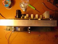
About the main heatsink, yes, I knew that someone would be curious with that weird heatsink. In fact, I use 2 heatsinks for my amp, for many reasons. First, I want to reuse the blac one( it's from a broken Japanese amp), but that heatsink is still small, and I also can't mount the module on that heatsink because its width is only about 60mm. So I decided to use another heatsink( the bright one), this one has 82mm width, so I can easily mount the amp modue on it, then assemble the 2 heatsink together with some bolts and thermal compound in such a way that you can see in the pictures. In addition, that heatsink has the fins along its length, and when I mount a DC fan under that heatsink, a tunnel for the air to flow is formed. Now I have a great weird heatsink! In fact, this heatsink worked very well when I tested my amp, and I fit well in the chassis(which is also reused from that broken amp).
At last, here's the sideview of my amp module, it will give you a clearer view, so you can understand how I use my heatsink, in case you can't understand my poor English.
Regards,
Duong
First, I'm very happy that you type my name correctly now
From what I understand, you said that the first time you view the image, you only saw the silk screen, right? Maybe there was something wrong when I posted the images, because after I had exported the image, I didn't found anything wrong, all the images were OK, the layout view had the tracks in red, the silk screen in white and black background, I really don't know what happened with the image. I will attach another layout (in black and grey like quasi) to check if the prob happen again.Maybe I should use pdf file like quasi too, but sadly my software doesn't allow posting image to pdf file, so I would need another software to change the image from gif or bmp file to pdf file, what a pain,if you know me better, you would see that I'm a lazy guy.
About the resolution of the image, I was very surprise as you said that the resolution of the image is only 72dpi, not 300dpi, because when I export my image, I can choose the resolution, from 100dpi to 600dpi. I will check again to see if my software has prob.
Thanks for your advice about GIMP,I will try it later, but I'm using ACDSee now, and I think it's enough for me now.
Thanks again for your praise about the driver heatsink, but I think I will replace it when I find a better one, because that heatsink is quite hot under normal condition.I also have some heatsink like Shawn's( Hi Shawn, thanks for your offer), but I'm afraid they aren't better than the one I'm using now.
About the res and the inductor of the Zobel network,I didnt have the inductor when I was drawing the board, so I put them seperate to be sure that all of them have enough space on the board( the 5W res may not fit inside some small inductor)
About the main heatsink, yes, I knew that someone would be curious with that weird heatsink. In fact, I use 2 heatsinks for my amp, for many reasons. First, I want to reuse the blac one( it's from a broken Japanese amp), but that heatsink is still small, and I also can't mount the module on that heatsink because its width is only about 60mm. So I decided to use another heatsink( the bright one), this one has 82mm width, so I can easily mount the amp modue on it, then assemble the 2 heatsink together with some bolts and thermal compound in such a way that you can see in the pictures. In addition, that heatsink has the fins along its length, and when I mount a DC fan under that heatsink, a tunnel for the air to flow is formed. Now I have a great weird heatsink! In fact, this heatsink worked very well when I tested my amp, and I fit well in the chassis(which is also reused from that broken amp).
At last, here's the sideview of my amp module, it will give you a clearer view, so you can understand how I use my heatsink, in case you can't understand my poor English.
Regards,
Duong
Attachments
Hi Hoang,
when setting up the amplifier, you should
1. remove all loads from the output.
2. insert a shorting plug into the input RCA.
3. adjust the DC output offset.
4. adjust the output stage quiescent current.
repeat 3 & 4 until conditions stabilise. This will take longer than 10minutes for the heatsink to warm up.
Switch off and allow all to go cold, do not make any adjustments.
Power up and recheck the DC offset and output bias from cold and monitor what it does as the amp warms up.
Did the DC offset and bias current behave as the amp went from cold to warm?
Now connect your normal source and check DC offset again.
Any change here indicates DC coming from your source. Fix the source if error is significant.
Now it's safe to connect your speakers and try some music.
Hi Duong
If your amp module works (amplifies signal cleanly) then I would go ahead and build the next module. This way you can compare differences between the two and track down the problem of the varying DC offset. You could try changing VR1 and VR2.
VR1 is used to compensate for component tolerances elswhere so the voltage across it may not be 0mV but something else.
The other voltages you have measured tell me that your amp is working fine. Can you please measure the voltage across R22.
Also post the voltages for R12 and R15.
Cheers
Toshiba and quasi
2SK1530’s or 2SK2698’s or both...or none?
Are these devices good or does Toshiba have something better. I'm talking about current offering not end of life products or old NOS.
I have a Toshiba connection coming through and with 10 or 20 pc sample order I can take what ever I want. I was looking a few weeks ago but I'm now distracted by work. I would much like your opinion(s) if yee have time.
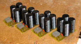
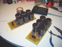
I purchased the software Quasi used to layout the Quatro PCB's. I always liked his hour glass figures I'll get it in a week or so. I renewed Q's PCB layout for his power supply to handle 60,000uF per Audio Channel of amp. I switched the PCB to accept single "inline" bridge rectifiers with standard leads. I will supply it with 30-0-30 VAC x 1.414 = Approx +/_ 40VDC off of 400 VA toroids hand wound or perhaps from Plitron. Depends how long I take to get ready for them. Six FETs per channel.
I am not happy with regular style case so I am looking for something more artistic. I will try to pull the FETs off the main PCBs and onto their own. Yes Quasi, I too have little time! I'll get it done but I will need more time. Perhaps if I write this post some time able folk will get interested and beat me to it .
Back to 3D CAD images of cement and brick...
Shawn.
2SK1530’s or 2SK2698’s or both...or none?
Are these devices good or does Toshiba have something better. I'm talking about current offering not end of life products or old NOS.
I have a Toshiba connection coming through and with 10 or 20 pc sample order I can take what ever I want. I was looking a few weeks ago but I'm now distracted by work. I would much like your opinion(s) if yee have time.
I purchased the software Quasi used to layout the Quatro PCB's. I always liked his hour glass figures
I'll get it in a week or so. I renewed Q's PCB layout for his power supply to handle 60,000uF per Audio Channel of amp. I switched the PCB to accept single "inline" bridge rectifiers with standard leads. I will supply it with 30-0-30 VAC x 1.414 = Approx +/_ 40VDC off of 400 VA toroids hand wound or perhaps from Plitron. Depends how long I take to get ready for them. Six FETs per channel.I am not happy with regular style case so I am looking for something more artistic. I will try to pull the FETs off the main PCBs and onto their own. Yes Quasi, I too have little time! I'll get it done but I will need more time. Perhaps if I write this post some time able folk will get interested and beat me to it
.Back to 3D CAD images of cement and brick...
Shawn.
minimizing offset
Hi,
DC on the output of any PA should be as low as possible. Its value largely depends on how well the input differential pair is matched. Matching Hfe at say under 100uV base current as in most multimiters is not enough. One should match well Ic currents under given circuit operational base current. Although it may seem complicated there is a very simple way around it.
Treat B-E junction as a diode - collector not connected - and put resistor R in a tested transistor base. Then connect a DC source (eg.battery) of about 10-15V between base resistor and emitter. Choose R value from a well know formula: R=U/i where i=base current as in the actual differential pair (in PA). Measurement accuracy of the voltage drop across the junction should not be worse than 1mV - say 100uV resolution is nice.
So repeat test with as many transistors you have, then choose those, which have close enough junction voltage drop. Then meaure their Hfe (ideally at the same base current) and choose those, which have the closest Hfe.
cheers,
Hi,
DC on the output of any PA should be as low as possible. Its value largely depends on how well the input differential pair is matched. Matching Hfe at say under 100uV base current as in most multimiters is not enough. One should match well Ic currents under given circuit operational base current. Although it may seem complicated there is a very simple way around it.
Treat B-E junction as a diode - collector not connected - and put resistor R in a tested transistor base. Then connect a DC source (eg.battery) of about 10-15V between base resistor and emitter. Choose R value from a well know formula: R=U/i where i=base current as in the actual differential pair (in PA). Measurement accuracy of the voltage drop across the junction should not be worse than 1mV - say 100uV resolution is nice.
So repeat test with as many transistors you have, then choose those, which have close enough junction voltage drop. Then meaure their Hfe (ideally at the same base current) and choose those, which have the closest Hfe.
cheers,
Hi Tomwaits,
2sk1530 is a nice audio FET.
It has slightly more current (Id) and slightly more power than a lateral FET, but well below the potential offered by the vertical FETs.
It also has an intermediate Vgs between vert and lat.
It seems to me that it is a halfway house, although technically I believe it is classified as a Vertical FET.
Re: Tomwaits
Abacom
sPlan & Sprint-Layout
Cheers.
ppcblaster said:What Software did you buy that Quasi used?
Abacom
sPlan & Sprint-Layout
Cheers.
- Home
- Amplifiers
- Solid State
- Power amp under development