Thats a pretty big heat sink for those bridge rectifiers. Why not turn the heat sinks around and keep all your wiring on the inside. ?
Hi,
All mechanical parts came from industrial rubbish, so they are little damage and not esthetical tip-top. I painted heatsink in black but i don't want they apparent from outside casing. For rectifier bridge, the heatsink can from rubbish too, it just pretty in dimension to fit at this place. I made 4 hole per main heatsink to pass through supply/gnd/out put wire.
Marc
thats a very good looking setup IDEFIXES but dont you think that your heat sink is way too much? does NMOS200 really required heatsink that big?but nice amp really.")
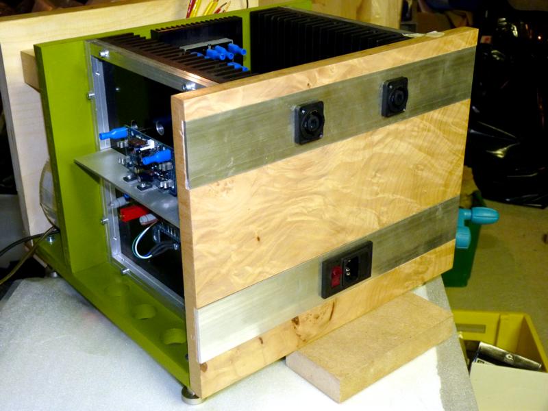
Yes it's overkill for NMOS200 but as i said previously, i don't pay for those heatsink, they are coming from industrial rubbish where i found 9 of them. They visualy a little bit damage but whith a little work on them and little bit paint they are good for diy project.
Marc
hi quasi...
I have build the nmos 200 with a +-25V rails and adjust some resistors values to suit up tha current feeds. It's a good amp but i need a more powerful version of the amp like the Nmos350 but my problem is the trafo that i have has a single secondary winding at 100vac, 1000VA.
So,how can we modify the nmos 350 to run on a single rail voltage of 140(just like +-70v) and put a output coupling capacitor. I am no designer just a builder.. your help is highly appreciated...
My NMOS200
my NMOS200 is working without any problem, initial test indicate that amp is in good condition from offset voltage to idle current, audio is clear with input from a cd player without preamp or tone control, I used +- 50 volts on it,I will soon build the 2nd channel , my NMOS 350 is having a problem with idle current adjustment, my plan to change all mosfet with 2sk1530 instead of using the irfp450 just like what I used with my NMOS 200, attached is the picture of initial test.
my NMOS200 is working without any problem, initial test indicate that amp is in good condition from offset voltage to idle current, audio is clear with input from a cd player without preamp or tone control, I used +- 50 volts on it,I will soon build the 2nd channel , my NMOS 350 is having a problem with idle current adjustment, my plan to change all mosfet with 2sk1530 instead of using the irfp450 just like what I used with my NMOS 200, attached is the picture of initial test.
Attachments


 Image fixed.
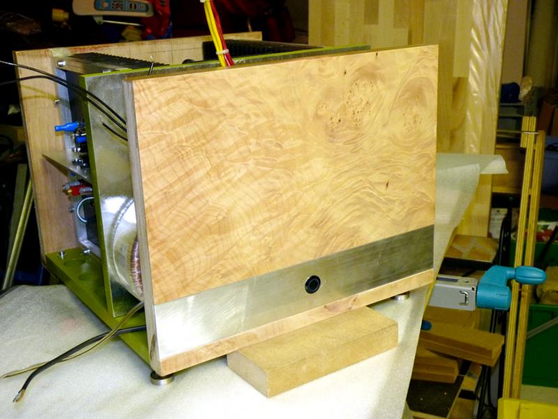
Sorry for my english, i am from Russia. Can i use this circuit, or exist better?
An externally hosted image should be here but it was not working when we last tested it.
Sorry for my english, i am from Russia. Can i use this circuit, or exist better?An externally hosted image should be here but it was not working when we last tested it.
hi SaMaHa
this is the final sch you can check this on his site
http://sites.google.com/site/quasisdiyaudiosite/home
regards
ravs
be a vegeterian........
Ha-ha, yes, i am from KGB.
On yours that who from Russia that KGB? How to place drawing?
Second attempt:
RapidShare: 1-CLICK Web hosting - Easy Filehosting
On yours that who from Russia that KGB? How to place drawing?
Second attempt:
RapidShare: 1-CLICK Web hosting - Easy Filehosting

Nmos350 Mk2 mod
Hi everybody!
It’s my first post here. Don’t shoot to me…
I modified Quasi’s Nmos350 Mk2 scheme and made PCB for this mod.
Here it’s.
I use small 0,6 W metal film resistors. Bipolar transistors are the same like on original scheme (I have usable only BD139/140 in my EAGLE library) except T9 – there is BD139 (TO126) and MOSFET transistors are IRF640. JP1 is there because I wont to try an additionally power supply like Upupa Epops in his great MOSFET amplifiers DPA3XX (post #164).
What’s yours opinion? Is this PCB correct (ground and component location...)?
Thanks.
Attachments


- Home
- Amplifiers
- Solid State
- Power amp under development