Hi,
The load: IRFP250
I calculated 1 amp drive current based on 100nC gate charge for 10Mhz. Yes? This is for a PWM application.
That should turn the sucker on nice and fast in the worst case I thought.
Now then..for the driver transistor...
After many hours of searching, I came up with the zetex FCX1149A, which is identical to their ZTX1149A, different case, handles twice the dissipation, slightly better Hfe.
I chose this one for it's ultra high beta and current rating, I can't go with a darlington as it would leave me with too high a base current requirement.
I couldnt' get it to work very well at all....couldn't figure out why it was switching so poorly..
So I stripped everything else away (I'm in spice land), and just tried switching the driver transistor through a 1 amp resistive load of 11ohms.
It switches so slowly the best I get is a sort of triangle wave out of it, even though I get the current I want, it's useless switching so slowly.
Ft is 135Mhz according to the data sheet, Ton=150ns Toff=270ns. Output capacitance 50pF. It should be able to handle a 1Mhz frequency I thought....it doesn't.....it doesnt' even handle half of that well.
What did I do wrong in the selection process, I thought this would work great.
I need some input here because if I can't select them better than that....may as well give up now.
Thanks
Chris
Hi,
The mere fact you asked me that tells me my selection wasn't all that bad?
I set the circuit back up as the test switch, 2n5401n handles this same circuit far better....only can't get 1 amp out of it. Strange power scheme is because of how the prior circuit was..
Thanks
Chris
The mere fact you asked me that tells me my selection wasn't all that bad?
I set the circuit back up as the test switch, 2n5401n handles this same circuit far better....only can't get 1 amp out of it. Strange power scheme is because of how the prior circuit was..
Thanks
Chris
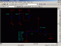
Attachments
OK, question: you are assuming that the puls generator floats atop the negrail. Did you check that? Many simulators *automagically* assume that any source is sitting on ground. Try to do it with all those voltage sources deleted, the puls generator against ground, the collector resistor to ground, just a pos battery for the emitter supply. And that 1.1k in the base lead doesn't help either, 50 ohms is better if you want just to test the transistor.
Jan Didden
Jan Didden
classd4sure!
- At fT transistors has 0dB current gain.
- BJT's switches off veeery slow, if they were saturated. Saturation must be avoided. Check out shottky-transistor!
- 1 A is not enough for 10MHz, since it has to turn on, and turn off during a period! 1/(100ns+100ns)=5 MHz.
- The charge must be loaded to, or sinked from gate at Ugs=4...5V. At this voltage only 0,4A flows on 11 ohm.
- This problem is already solved. Solution is MIC4421, or UCC27321 9A MOSFET drivers (for example).
- Maybe you should choose faster MOSFET. For example IRFB31N20D, W34NB20, or under 150V: FDP2552...
I hope I helped You!
Hi,
Yes, that's a very fair question, and a good one...I saw it comming. I know multisim would never accept that ..this program does, I of course, did check that.
The reason I chose 1.1k..
Under these conditions I reasoned min Hfe according to the data sheet graph =200.
I used 100 for calculation...more than safe I thought.
so for the 10mA required at the base=1.1k....half of what "should" work. IRL...I'd take required base current X3..but this is spice, and I reasoned I had already left enough of a margin of error by using Hfe 100 instead of the 200 it actually should be.
Am I wrong? Looks like it..but why?
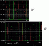
50Ohm or 1.1k ohm ....still gives me my 1 amp of course. I think the 1.1k should do a far better job of switching it though. I will attach a pic of the results given the same circuit with the two different base resistors driven at 500Khz and an easy duty cycle of 50%, I think you'll agree it's useless for PWM at even that slow a speed, even with the 50ohm.
At 50Ohm it measures 325n off delay, worse than the 270n it's rated at. It will have a baker clamp ...should I really have to overdrive it like this just to get it to fully switch? I would think not.
Regarding the 10Mhz, working frequency of this circuit will be around 350k PWM full modulation. So again it seemed to me that 10Mhz was enough of a margin to calculate required drive current with, to allow it to swith on /off in 100ns.
Pafi, You are correct Sir, the gate resistor calculates to 5ohms in my actual circuit, the reason it's 11 ohms here is because it's not the actual circuit. 11V/1amp load =11ohm..just to see how good it can switch this current.
Jan, that's a respectable looking wave, do you only get 200 to 500mA out of it? Too bad..Guess that's not my transistor either.
Thanks
Chris
PS: If this makes no sense ...I'm simply burnt....and will edit later")
Yes, that's a very fair question, and a good one...I saw it comming. I know multisim would never accept that ..this program does, I of course, did check that.
The reason I chose 1.1k..
Under these conditions I reasoned min Hfe according to the data sheet graph =200.
I used 100 for calculation...more than safe I thought.
so for the 10mA required at the base=1.1k....half of what "should" work. IRL...I'd take required base current X3..but this is spice, and I reasoned I had already left enough of a margin of error by using Hfe 100 instead of the 200 it actually should be.
Am I wrong? Looks like it..but why?
50Ohm or 1.1k ohm ....still gives me my 1 amp of course. I think the 1.1k should do a far better job of switching it though. I will attach a pic of the results given the same circuit with the two different base resistors driven at 500Khz and an easy duty cycle of 50%, I think you'll agree it's useless for PWM at even that slow a speed, even with the 50ohm.
At 50Ohm it measures 325n off delay, worse than the 270n it's rated at. It will have a baker clamp ...should I really have to overdrive it like this just to get it to fully switch? I would think not.
Regarding the 10Mhz, working frequency of this circuit will be around 350k PWM full modulation. So again it seemed to me that 10Mhz was enough of a margin to calculate required drive current with, to allow it to swith on /off in 100ns.
Pafi, You are correct Sir, the gate resistor calculates to 5ohms in my actual circuit, the reason it's 11 ohms here is because it's not the actual circuit. 11V/1amp load =11ohm..just to see how good it can switch this current.
Jan, that's a respectable looking wave, do you only get 200 to 500mA out of it? Too bad..Guess that's not my transistor either.
Thanks
Chris
PS: If this makes no sense ...I'm simply burnt....and will edit later
Attachments
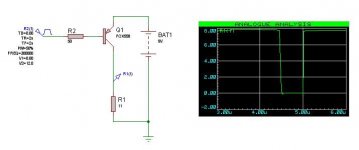
Well, my graph showes 8V across 11 ohms from a 9V battery, which for a small signal transistor is good (VCEsat=1V), and the switching speeds show that it works. It's really a trivial cct of course. If it doesn't work in your case, it's not the transistor, believe me.
Did you try with the puls gen against ground? How did you check that the floating puls gen works?
Jan Didden
Did you try with the puls gen against ground? How did you check that the floating puls gen works?
Jan Didden
Hi Chris,
I do not know if your requirements are really serious (10Mhz switching), but presuming that they are I do not think you have chosen the right way. I have been simulating switching designs almost to death, and I have found out that component models usually do not work very well in Spice. Sometimes FET models lack package parasitic inductances etc. So for longer simulations (over many switching cycles) I prefer to use S (switch element).
If your requirements are really 10MHz, you are candidate for IXYS RF (former Directed Energy) FETs. Also for 10Mhz switching, you would not use classic drive circuit, but some kind of resonant driver. Those usually use gate inductor instead of gate resistor. Such drivers have low losses, since they conserve energy in resonant circuit instead of dissipating it in the gate resistor. There are many variants of such designs, and I may try and find some examples, if you are interested.
Best regards,
Jaka Racman
The problem is saturation (at 50 ohm drive), and insufficient basis current (at 1k).
Look at this: http://www.hszk.bme.hu/~sp215/elektro/stuff.gif
Or this one: http://www.hszk.bme.hu/~sp215/elektro/stuff2.gif
The 10 nF is simulating the gate capacitance.
But why don't You use driver IC?
Look at this: http://www.hszk.bme.hu/~sp215/elektro/stuff.gif
Or this one: http://www.hszk.bme.hu/~sp215/elektro/stuff2.gif
The 10 nF is simulating the gate capacitance.
But why don't You use driver IC?
janneman said:Well, my graph showes 8V across 11 ohms from a 9V battery, which for a small signal transistor is good (VCEsat=1V), and the switching speeds show that it works. It's really a trivial cct of course. If it doesn't work in your case, it's not the transistor, believe me.
Did you try with the puls gen against ground? How did you check that the floating puls gen works?
Jan Didden
Yeah I said it looks good, but it doesn't get the job of sourcing an amp done, is all that I meant. This isn't government work
According to my simulation, you only get 375mA out of it.The floating pulse gen. works..it's the green line in the graphs I posted.
Thanks,
Chris.
Jaka Racman said:Hi Chris,
I do not know if your requirements are really serious (10Mhz switching), but presuming that they are I do not think you have chosen the right way. I have been simulating switching designs almost to death, and I have found out that component models usually do not work very well in Spice. Sometimes FET models lack package parasitic inductances etc. So for longer simulations (over many switching cycles) I prefer to use S (switch element).
If your requirements are really 10MHz, you are candidate for IXYS RF (former Directed Energy) FETs. Also for 10Mhz switching, you would not use classic drive circuit, but some kind of resonant driver. Those usually use gate inductor instead of gate resistor. Such drivers have low losses, since they conserve energy in resonant circuit instead of dissipating it in the gate resistor. There are many variants of such designs, and I may try and find some examples, if you are interested.
Best regards,
Jaka Racman
Hi Jaka,
Yeah I've studied IXY's app notes thoroughly back when I was dreaming of switching DSD to the load directly at high power..and came to the conclusion that kind of a circuit is a bit out of my grasp at this point, but its' good reading!
I make no secret of the fact I'm working on a high power UCD circuit....500 watts continuous is my goal for the half bridge. I won't build what I can't simulate..
I've had the exact circuit simulate a THD of .2% with no extra filtering using the 1N5401's to drive these very mosfets..but I did calculate 1 amp at 10Mhz in order to ensure very snappy switching at the modulation extremes...1%.....99%...how fast would be required? The idea behind that being a good margin of safety for the math, if it could switch on at 100ns, it would work great at 350khz or so...and doubling up the power mosfets would have been trivial with 1 amp drive.
Thought the zetex would be better. In the circuit itself it's just ugly, and the simple switch test I did shows it rather slow for some reason.
The S-switches...I'll have to figure out how to use those one day..would make the proof of concept playing around alot easier.
There's a few other glaring problems that still need working out, but I thought I'd try and nail down the output aspect of it first.
Thanks
Chris.
Pafi said:The problem is saturation (at 50 ohm drive), and insufficient basis current (at 1k).
Look at this: http://www.hszk.bme.hu/~sp215/elektro/stuff.gif
Or this one: http://www.hszk.bme.hu/~sp215/elektro/stuff2.gif
The 10 nF is simulating the gate capacitance.
But why don't You use driver IC?
Hi,
Two good reasons, my lab consists of my computer..they're impossible to simulate, and rarely find models of them, the driver you mentioned isn't one I've seen before, but it sure looks promissing.
The main reason is...it goes against the UCD design..of symetrical non saturated very fast transistors. I don't think a driver chip would be an improvement on that...even if I could get a working simulation going of it.
Once I get the simulations as perfect as I can, I plan on just prototyping it up and watching it smoke
I don't even have a scope
Thanks alot for your input, it's most welcome and right on the money.
I don't think my calculations are off in my little switch example..and I did use half the beta to calculate with than its' rated for at that current...So I thought it would work...but since it doesn't...it seems to fully switch with a base resistance of around 330....and will have a baker clamp..
Maybe I'll play with it more later
Cheers
Chris
Chris!
Please tell me what does "UCD design" mean! I'm not very good at terminology in English!
"I don't think a driver chip would be an improvement on that"
These are technically perfect, I think:
Features
• BiCMOS/DMOS Construction
• Latch-Up Proof: Fully Isolated Process is Inherently
Immune to Any Latch-up.
• Input Will Withstand Negative Swing of Up to 5V
• Matched Rise and Fall Times ............................... 25ns
• High Peak Output Current .............................. 9A Peak
• Wide Operating Range .............................. 4.5V to 18V
• High Capacitive Load Drive ........................... 47,000pF
• Low Delay Time ........................................... 30ns Typ.
• Logic High Input for Any Voltage from 2.4V to VS
• Low Equivalent Input Capacitance (typ) .................7pF
• Low Supply Current .............. 450µA With Logic 1 Input
• Low Output Impedance ........................................ 1.5Ω
• Output Voltage Swing to Within 25mV of GND or VS
It's in SO-8 package. Do we need more? You can replace it with ideal comparator+1,5ohm resistor in simulation!
But if you insist the simulation, then take this: http://www.hszk.bme.hu/~sp215/elektro/stuff3.gif
I've used this untill I met MIC4421. (But with FDT457-458)
Note: driver dissipation should not exceed one of the output device!
P.S.: Scope, and Laplace-transformation are the best friend of engineer!
Please tell me what does "UCD design" mean! I'm not very good at terminology in English!
"I don't think a driver chip would be an improvement on that"
These are technically perfect, I think:
Features
• BiCMOS/DMOS Construction
• Latch-Up Proof: Fully Isolated Process is Inherently
Immune to Any Latch-up.
• Input Will Withstand Negative Swing of Up to 5V
• Matched Rise and Fall Times ............................... 25ns
• High Peak Output Current .............................. 9A Peak
• Wide Operating Range .............................. 4.5V to 18V
• High Capacitive Load Drive ........................... 47,000pF
• Low Delay Time ........................................... 30ns Typ.
• Logic High Input for Any Voltage from 2.4V to VS
• Low Equivalent Input Capacitance (typ) .................7pF
• Low Supply Current .............. 450µA With Logic 1 Input
• Low Output Impedance ........................................ 1.5Ω
• Output Voltage Swing to Within 25mV of GND or VS
It's in SO-8 package. Do we need more?
You can replace it with ideal comparator+1,5ohm resistor in simulation!But if you insist the simulation, then take this: http://www.hszk.bme.hu/~sp215/elektro/stuff3.gif
I've used this untill I met MIC4421. (But with FDT457-458)
Note: driver dissipation should not exceed one of the output device!
P.S.: Scope, and Laplace-transformation are the best friend of engineer!
Hi Chris,
now that I know your intentions you have my best wishes. I have been doing SMPS design professionally for many years, but I would not dare to design anything switching without a scope, unless using a previously proven design or blocks. It might be a professional deformation, but I feel naked without a scope. On the other hand I know a very bright guy (he is now a university professor, but he could teach some professors when he was still a student) that can do gigahertz ham radio designs only with theory and analog multimeter. Maybe you could post your schematics for comment before you actually start building?
Best regards,
Jaka Racman
Hi,
Pafi, thanks for all your help.
UCD stands for "Universal Class D" formely "Ultimate Class D" and is the best class D topology out there today (mueta doesn't count yet, and probably won't sound as good either)..
I will find you the link to the patent info so you too can see it's elegant beauty.
Bruno's UCD patent
Have a look at that and you'll understand why I don't want to use a driver chip. Nothing is stopping me from doing it, but I dont' think it would be as good as what's on the patent.
Believe me guys, I'd love to have a scope, and for this type of project, naked without it is spot on, probably even more so like trying to land a jet on an aircraft carrier in the middle of a winter storm with half the landing gear down. Why should that stop me from trying?
I'll P2P a prototype, power it with +-12 regulated 1 amp...see what smokes....tweak it a little..if it works..I'll work on the power supply...Maybe I can take a local repair shop hostage for a few hours and use theirs? See what happens.
In the meantime I can perfect the design as much as I can on spice, the better it gets the more confidence I'll have with making a prototype. If the prototype works half decent..(it will either smoke, play, or something in between) I'll make the pcb..hopefully by then I'll have a scope at least anyway.
It's a learning experience, keeps me busy, and if I should wind up with a great amp when it's all said and done..I'll be happy.
As far as posting the schematic goes, once I've taken it as far as I can I'd be happy to. I'd only be laughed at if I posted what I had now..
Thanks for the kind words and help, I won't be giving up anytime soon.
Do you guys think I made the right choice of transistor after all?
I'll be looking up the ones Pafi mentioned later once I've had some rest.
I reaaaally should have a scope to experiment with what makes everything work best for this sort of thing..That will have to come later, but there's no reason why I can't have a good design of it now. I have a dead monitor I keep looking at sideways hmmmmm.
Take care, and thanks again.
Chris
I draw this some time ago thinking in fast MOSFET drive for low voltage SMPS, but I think there are also some useful ideas for class D
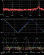
This shows the latter circuit in action, driving an IRFZ48V from simple BC337/327 bipolars and 10ohm Rg in a push-pull circuit [turn-off from conducting 60A or so]. Leftmost trace is Vgs at 5V/div [I use 18V drive], rightmost trace is Vds at 10V/div, time is 200ns/div and gate is discharged in less than 120ns. This also shows that high current MOSFETs are not perfect and suffer some degree of 'current tail' and 'storage time' effects as opposed to what common wisdom says
In the other hand, with ZTX851/951 bipolars configured as a simple class-B buffer driven from paralell CMOS buffers I've got performances as good as 50ns or less charge/discharge times for an IRFP460 switching 300V [including 'miller' capacitance effects, very noticeable at these high voltages]
An externally hosted image should be here but it was not working when we last tested it.
This shows the latter circuit in action, driving an IRFZ48V from simple BC337/327 bipolars and 10ohm Rg in a push-pull circuit [turn-off from conducting 60A or so]. Leftmost trace is Vgs at 5V/div [I use 18V drive], rightmost trace is Vds at 10V/div, time is 200ns/div and gate is discharged in less than 120ns. This also shows that high current MOSFETs are not perfect and suffer some degree of 'current tail' and 'storage time' effects as opposed to what common wisdom says
An externally hosted image should be here but it was not working when we last tested it.
In the other hand, with ZTX851/951 bipolars configured as a simple class-B buffer driven from paralell CMOS buffers I've got performances as good as 50ns or less charge/discharge times for an IRFP460 switching 300V [including 'miller' capacitance effects, very noticeable at these high voltages]
- Status
- This old topic is closed. If you want to reopen this topic, contact a moderator using the "Report Post" button.
- Home
- Amplifiers
- Class D
- poor switching