Of course both layouts are very tidy and reasonably compact, they reflect some experience but no attention to details like PCB and component parasitics. Furthermore, I know quite well that laying out boards is very time consuming (I'm currently doing several layouts involving two layers, ground planes and SMD).
However, since you always seem to want to be one step ahead by using the best components and topologies on your amplifiers, why not being one step ahead with PCB layouts too?")
BTW: I forgot to mention that the output devices should ideally be placed close to the supply decoupling capacitors too.
However, since you always seem to want to be one step ahead by using the best components and topologies on your amplifiers, why not being one step ahead with PCB layouts too?
BTW: I forgot to mention that the output devices should ideally be placed close to the supply decoupling capacitors too.
Hi again Eva,
I'm afraid I'm guilty of knowing that the PCB layout will not make a huge difference to the final outcome for these simple amps.
I'm also guilty of not knowing all (or even some) of the rules and tricks that can be used to improve upon the layout. The things that are routine and second nature to someone working in their own field of expertise are not obvious to us that are not.
Yes, layout is very time consuming, even for these simple amps. To have a better understanding of the important choices regarding parts placement and such beforehand would be a good head start, so I'm listening to all of the advice I get.
dear eva ....
i actually lost my sleep over this .....
this is what i come up with
------as we said my pcb has to be symmetric( my ""thingy ''')
------ then pcb has to be usefull ( no special heat sink should be required)
------ amp like that should easily fit in a 2U sassi ( use of a 3U sassi is out of the question )
------ there is another must, that psu caps have to be located on board
------and finally pcb has to be kinda versatile so its a drop in replacement to destroyed amps ( mean comapct and easy to work with )
then we have some of your rules
-----one side includes power section caps and power and output terminals, decoupling next to eachother and power transistors ,and then on the other side has to be the small stuff
------mean while star ground is to be preserved
------ and ground traces have to be as small is possible ...
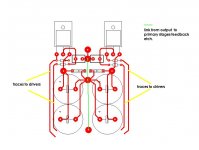
the only thing that i could come up with is this basic schematic BUT !!!!
---------as you can see there is onegreen link that will develop the output to the small stuff area for feedback zobel and so on
---------and also the 2 traces marked with yellow will be used to send signal from the drivers to output section
question is : if you agree with the traces of the drivers runing like this next to power supply then i will proceed with the rest of the pcb
sorry for the extensive explanation of the principal but i thought that a summary will put the thread back in the original track
i actually lost my sleep over this .....
this is what i come up with
------as we said my pcb has to be symmetric( my ""thingy ''')
------ then pcb has to be usefull ( no special heat sink should be required)
------ amp like that should easily fit in a 2U sassi ( use of a 3U sassi is out of the question )
------ there is another must, that psu caps have to be located on board
------and finally pcb has to be kinda versatile so its a drop in replacement to destroyed amps ( mean comapct and easy to work with )
then we have some of your rules
-----one side includes power section caps and power and output terminals, decoupling next to eachother and power transistors ,and then on the other side has to be the small stuff
------mean while star ground is to be preserved
------ and ground traces have to be as small is possible ...
the only thing that i could come up with is this basic schematic BUT !!!!
---------as you can see there is onegreen link that will develop the output to the small stuff area for feedback zobel and so on
---------and also the 2 traces marked with yellow will be used to send signal from the drivers to output section
question is : if you agree with the traces of the drivers runing like this next to power supply then i will proceed with the rest of the pcb
sorry for the extensive explanation of the principal but i thought that a summary will put the thread back in the original track
Attachments
Me again 
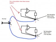
Two perfect amplifiers. Each on it's own behaves perfectly. Imagine the top one is pushing 5 amps through the load. That develops a volt drop along "A" and "B". Not a problem in itself. If it's music the volt drop will have all the "capacitor current" disturbance feeding into this line. Still not a problem.
The problem is this. The two input grounds of the top and bottom amp are not at the same potential. And these have to connect together at some point.
Do you see what I mean You have no one true reference point. Returning the speaker off PCB is a must. So to is the ground return of the large caps you have on the PCB. The input ground which carries no significant current also has to be refered back to the main star point.
Two perfect amplifiers. Each on it's own behaves perfectly. Imagine the top one is pushing 5 amps through the load. That develops a volt drop along "A" and "B". Not a problem in itself. If it's music the volt drop will have all the "capacitor current" disturbance feeding into this line. Still not a problem.
The problem is this. The two input grounds of the top and bottom amp are not at the same potential. And these have to connect together at some point.
Do you see what I mean
You have no one true reference point. Returning the speaker off PCB is a must. So to is the ground return of the large caps you have on the PCB. The input ground which carries no significant current also has to be refered back to the main star point.Attachments
Hi Sakis
Long driver traces are usually better than long power traces, althouth splitting a CFP that way is not a good idea, it's better to split between the VAS and the FCP. But why are you maing the power supply secion so tall? You could make it wider and less tall by laying out the capacitors horizontally to shorten driver traces.
Also, why are you not using the space above the power transistors? Placing them in one of the borders of the PCB is not the optimum solution, why not placing them in the middle and bolting them to the heatsink through the PCB (sandwitching)? These same screws will hold the PCB to the heatsink too, and in case of TO-220 or TO-218 devices electrical isolation of the screws will come for free. I do most of my power layouts that way, which sandwitched power devices spread all over the PCB.
Another important idea: Why don't you use a vertical daughter board for the small signal circuits? this really saves space, makes the layout easier and helps when you have to pack several amplifier channels, preamplifier, housekeeping, etc.. in a single PCB.
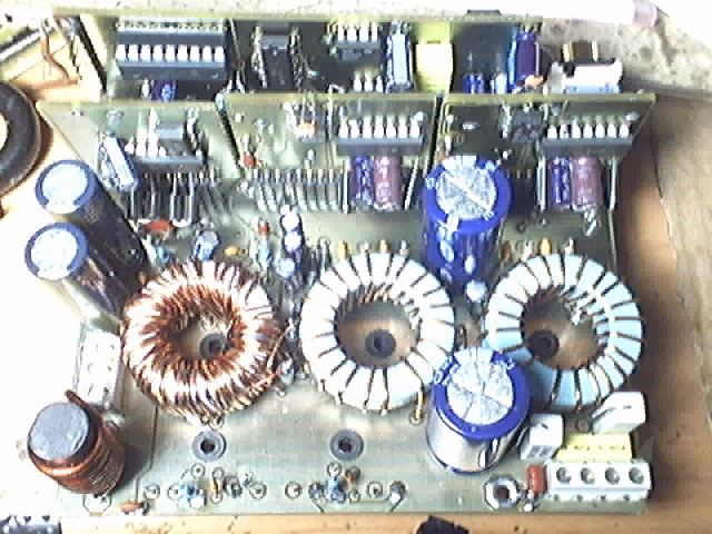
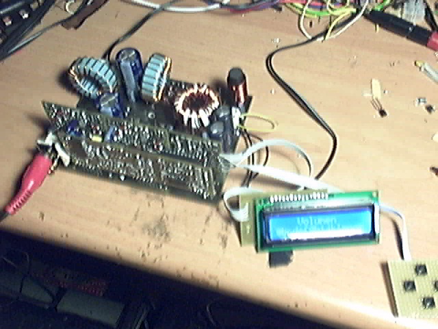
For example, see my little 2x120W class-D full range car amplifier (with built in +/-35V power supply). Notice the holes for screws for each pair of TO-220. It measures 17cm x 10cm x 4cm. The design is modular using daughter boards. :
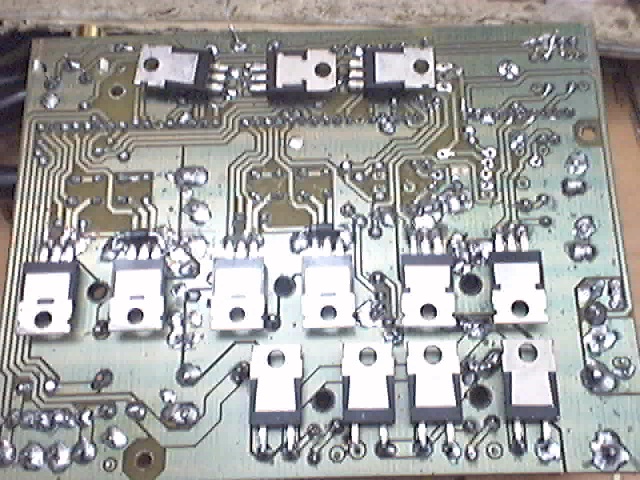
Well, actually you would require heavier clamping of the power devices since your amplifier is class AB and produces far more heat (this little amplifier plays full volume with no heatsink and you can still keep your finger on the transistors without burning yourself). This may be achieved with the help of metal rails or large washers to avoid the PCB bending too much. However, note that I'm using this same mounting scheme for 2400W sinewave inverters and class D where transistor dissipation is not so low and it's working fine too.
Edit: Oh, concerning the grounds, keeping separate signal and power grounds is a must for multichannel applications, otherwise cross-talk and humm and buzz would be severely degraded.
Long driver traces are usually better than long power traces, althouth splitting a CFP that way is not a good idea, it's better to split between the VAS and the FCP. But why are you maing the power supply secion so tall? You could make it wider and less tall by laying out the capacitors horizontally to shorten driver traces.
Also, why are you not using the space above the power transistors? Placing them in one of the borders of the PCB is not the optimum solution, why not placing them in the middle and bolting them to the heatsink through the PCB (sandwitching)? These same screws will hold the PCB to the heatsink too, and in case of TO-220 or TO-218 devices electrical isolation of the screws will come for free. I do most of my power layouts that way, which sandwitched power devices spread all over the PCB.
Another important idea: Why don't you use a vertical daughter board for the small signal circuits? this really saves space, makes the layout easier and helps when you have to pack several amplifier channels, preamplifier, housekeeping, etc.. in a single PCB.
For example, see my little 2x120W class-D full range car amplifier (with built in +/-35V power supply). Notice the holes for screws for each pair of TO-220. It measures 17cm x 10cm x 4cm. The design is modular using daughter boards. :
Well, actually you would require heavier clamping of the power devices since your amplifier is class AB and produces far more heat (this little amplifier plays full volume with no heatsink and you can still keep your finger on the transistors without burning yourself). This may be achieved with the help of metal rails or large washers to avoid the PCB bending too much. However, note that I'm using this same mounting scheme for 2400W sinewave inverters and class D where transistor dissipation is not so low and it's working fine too.
Edit: Oh, concerning the grounds, keeping separate signal and power grounds is a must for multichannel applications, otherwise cross-talk and humm and buzz would be severely degraded.
three connections from each amplifier to Audio Ground.Mooly said:The problem is this. The two input grounds of the top and bottom amp are not at the same potential. And these have to connect together at some point.
You have no one true reference point. Returning the speaker off PCB is a must. So to is the ground return of the large caps you have on the PCB. The input ground which carries no significant current also has to be referred back to the main star point.
1.) Signal Ground.
2.) Power Ground.
3.) Speaker return.
Keeping the PCB Signal Ground and the PCB Power Ground separate gives you the best chance to wire up your multi-channel amp correctly.
The feedback line/trace can come from the Speaker Out pad and between each of the cap pins all the way to the other end of the PCB.
I would try to get the route from output device to small decoupling cap to other small decoupling cap to output device even shorter than your present layout.
Disconnect the output collector feed from the V+ and V- pads. Instead connect the collectors to the nearer of the main smoothing caps. The charging pulses coming into the V+ & V- pads to the smoothing caps should be kept separate from the feed to any parts of the circuit.
1.) Signal Ground.
2.) Power Ground.
3.) Speaker return.
Maybe even a 4th. Zoble ground.(could be tacked on to speaker
return.)
Also , poking around in so many 5 and 7 channel HT receivers
I noticed that they use copper Bus bars above the board to
distribute the rails to each amp, separate ground traces for
zobles,inputs ,and small decoupling caps(one hell of a star!)
As this is similar to the P3A (CFP OP) it might be pickier
(oscillations) about
layout especially with certain OP device selections (high Ft)
also to keep Vbias "tight' you might want to mount your Vbias
and one of the drivers "back to back"(2 flat devices) for better temp.
compensation.
Good luck. a very simple, reliable amp if done right.
OS
well eva
Eva said:Hi Sakis
Long driver traces are usually better than long power traces, althouth splitting a CFP that way is not a good idea, it's better to split between the VAS and the FCP. But why are you maing the power supply secion so tall? You could make it wider and less tall by laying out the capacitors horizontally to shorten driver traces.
Also, why are you not using the space above the power transistors? Placing them in one of the borders of the PCB is not the optimum solution, why not placing them in the middle and bolting them to the heatsink through the PCB (sandwitching)? These same screws will hold the PCB to the heatsink too, and in case of TO-220 or TO-218 devices electrical isolation of the screws will come for free. I do most of my power layouts that way, which sandwitched power devices spread all over the PCB.
Another important idea: Why don't you use a vertical daughter board for the small signal circuits? this really saves space, makes the layout easier and helps when you have to pack several amplifier channels, preamplifier, housekeeping, etc.. in a single PCB.
For example, see my little 2x120W class-D full range car amplifier (with built in +/-35V power supply). Notice the holes for screws for each pair of TO-220. It measures 17cm x 10cm x 4cm. The design is modular using daughter boards. :
well eva ..it seems we are getting somewhere ... from all the above you are saying most of them conflig with the list of must that i placed above ......
the only thing that makes some sence is the piggy board.... which is something ive done before and i found very nice to use and covers all these needs we talked in this long thread .....
i ll work on it over the weekend and get back to you .....
as about all the advice i got regarding ground ....Andrew ... Mooly thank you very much about the usefull info ..... please let some time to end up the pcb issue and then we will come to ground issues as well ....thanks though
an important issue
this is the lay out of P3A
BUT!!!! this a project that i do for my private amusement .... this is a relaxation exercise for me
All the people above who mentioned the word P3a in there posts have been notified by private emails from me trying to explain that this effort is something that i do for me i have no intention to sell pcb or create any competition with rod's pcb .
the last thing i wanted to have is builders of P3A to jump in to this thread asking things or compairing pcb .....
the last thing i wanted someone to say is : ohhh that pcb is better than rod's
SO ..... i tryied to notify people that used the word P3A and it seems that we cannot keep a low profile about this .....
so i will ask rod to take a look on this thread and with your permission and if rod thinks that his business might be harmed from all that i will ask amoderator to close the thread permenatelly ....
i have greate respect for rod and his work and let us not forget that his sharing most of his work for free for all of us and it wouldnt be nice to harm him in any possible way ....
thanks for your atention
But rob elliot WANTS us to build this amp for our amusement/
education ,so you are doing right, sakis, we just want you
to be happy in your amusement ...instead of poor performance/
burning amps (which can be fun ,too)
I,ve carefully read the ESP site , rob wants us to build his circuits
as long as we acknowledge him and don't kill ourselves in
the process.
Ive seen a real P3A board and there is nothing special about it
(I think he is really stressing the P68 and the P3A is just a
simple hobbyist amp which he "borrowed" from an old design)
Have fun with a good simple amp which I know is public domain
,simply just don't call it a "P3A".
OS
MJL21193 said:The V- and input only appear to be close and the wires that leave the board from these two positions do not / would not run parallel.
The THD figure was a bit higher than the figure you quoted but certainly well below the threshold of audibility. I'll take it.
Practical mechanical layouts in high power audio amplifiers will always limit one to less than theoretically ideal PCB layouts.
But that not always matters too much or is the end of the world.
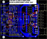
The not-so-serious design attached below measures ~0.001% THD-20; not so far removed from Edmond Stuart Microcap sim of ~0.0008%, eh?
The transistors are laid out in a line to mount on the moulded mounting tab of the Conrad heatsinks used.
The layout is split between the VAS and the triple EF output. Due to the fact that the transitional miller compensation used is tapped from the VAS collector the collector impedance at HF is at the ohm level. So, the layout is split at a low impedance point – an important consideration.
The output stage supply leads run from the filter capacitors are twisted and run underneath the heatsink mounting tab, but enter the PCB at (Shock! Horror!) opposite sides of the PCB. What really matters is that the small-signal stuff is well away and the power and small signal grounds are not messed/mixed up.
Cheers,
Glen
Attachments
If it's biased into class A, the supply currents are no longer chopped and the rails may be wired separately. Also, output stages involving switching are much more demanding on layout because they result in current spikes involving frequencies up to over 1Mhz.
Class A is the most forgiving operation mode because there is really nothing happening in the circuit above 20Khz, unlike in all other operation modes.
You could get very low THD figures operating on optimum biased class AB, but probably not with this layout. Part of the switching distortion is layout related.
Eva said:If it's biased into class A, the supply currents are no longer chopped and the rails may be wired separately. Also, output stages involving switching are much more demanding on layout because they result in current spikes involving frequencies up to over 1Mhz.
Class A is the most forgiving operation mode because there is really nothing happening in the circuit above 20Khz, unlike in all other operation modes.
You could get very low THD figures operating on optimum biased class AB, but probably not with this layout. Part of the switching distortion is layout related.
And how many "very low THD" class A / AB amplifier have you laid out and tested?
Class AB operation (much worse than optimal class B in terms of high switching currents) into 1/2 the rated load impedance yields a measured THD-20 of about 0.01%
Eva said:If it's biased into class A, the supply currents are no longer chopped and the rails may be wired separately. Also, output stages involving switching are much more demanding on layout because they result in current spikes involving frequencies up to over 1Mhz.
Class A is the most forgiving operation mode because there is really nothing happening in the circuit above 20Khz, unlike in all other operation modes.
You could get very low THD figures operating on optimum biased class AB, but probably not with this layout. Part of the switching distortion is layout related.
Virtually identical layout here (four output devices this time in a row, +/- supply wires connecting to opposites sides of the board, etc) :
http://www.siliconchip.com.au/cms/A_110797/printArticle.html
0.008% THD-20 200W ~optimal bias class B. I guess that isn't very low then.
Are you blind or what?
Supply rails are connected and laid out together through the center of the board, and decoupling capacitors are also placed together on the center.
This is a good layout, it more or less follows my guidelines. No wonder THD is low

Edit:
Note the quasi-ground-plane arrangement: The supply rail traces are on the top side while the speaker output and return traces are under them on the bottom side following the same path to reduce inductance and coupling to small signal circuits.
Supply rails are connected and laid out together through the center of the board, and decoupling capacitors are also placed together on the center.
This is a good layout, it more or less follows my guidelines. No wonder THD is low
Edit:
Note the quasi-ground-plane arrangement: The supply rail traces are on the top side while the speaker output and return traces are under them on the bottom side following the same path to reduce inductance and coupling to small signal circuits.
Eva said:Are you blind or what?
Supply rails are connected and laid out together through the center of the board, and decoupling capacitors are also placed together on the center.
My error, I was supposed to link to the Ultra LD MKI, which measures about the same:
http://www.siliconchip.com.au/cms/A_102322/article.html
- Status
- This old topic is closed. If you want to reopen this topic, contact a moderator using the "Report Post" button.
- Home
- Amplifiers
- Solid State
- please comment my pcb