I noticed the high resistor value in the signal path. I will
work on the circuit to see if this can be changed and
post the result here for suggestions.
On another matter, I never saw about the capacitor
type which are good for phono preamp mentioned
with circuits in the net. Are polyester good or polypropylene?
I am asking because if polypropylene then
I have a problem as I have to import them as well.
Not available locally in small quantity.
Thanks
Roushon.
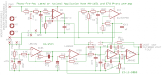
Hi, nice boards. What are the resistors to set the circuit gain and what's the formula to get their values? I'd like to maybe build this for a MM cart.
Hi, thanks! The circuit is for MC type cartridge. The gain
setting resistors are usual, that is the ones joining
the output of the individual opamp to their respective
-input and the resistors to the ground from their. I did not
do any calculation but followed the application notes. The
formula should be standard for opamps.
I am just finishing a similar board for MM type cartridge
based on this application notes and the circuit in Elliot
Sound Product page pointed out by Leon.
I still did not have time to work on the bugle preamp.
For the time being I would like to try the EPS one.
The single channel circuit/board for the MM type is
attached.
Will post the stereo preamp board soon. It is just
two such boards placing side by side but will have
single power entry.
Regards
Roushon
Attachments
Roushon, thank you very much. Originally I was also interested in building the Esp phono preamp but I got worried when I read "customary "flattening" of the curve at 50Hz has not been fully incorporated". I then looked else where. I wasn't sure if a bassy record would pose issues with the Esp stock. What opamps are you using with your Esp build?
Please post your thoughts on any of the three phono preamps when you're done with them. I'd love to read it.
Please post your thoughts on any of the three phono preamps when you're done with them. I'd love to read it.
I read that statement in ESP too, but not giving much thought to it as I do not have any experience with
phono preamp or record playing. Leon built it and
listened and I am following his suggestion.
The same opamps as in the circuit will be used. Although
ESP used 5532 (0r TL072). I think the ics in the circuit
are very good quality and made for phono stages only.
Edit: It just came to my mind that a bass enhanced signal will
be good in my case as I am playing on open baffle
speakers (self-made based on MJ Kings Design, the
thread on speakers forum (`suitable speakers' in multi-way))
Roushon.
Last edited:
Hi,
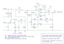
I must admit that from the first time I read the App-note I thought it to be a little weird, the way they treated the power supply voltages. I´d rather opt for a more classical approach. There are some new and fine voltage regulators out there (see BB/TI TPA7S-series) that could ease the design and probabely are even superior.
A second point deals with the position of the DC-Servos. The most critical stage regarding offset is the stage with the highest gain, usually the input stage. I´d place the DC-servo as close as possible to this stage to prevent offsets from influencing other stages too. C8 at the Input of IC3A prevents high offset voltage values, as does C4 in the second stage, so that the DC-Servo may either remain behind the second linear gain stage IC3b or could be omitted with alltogether. If You want to omit with large Electrolytic caps the Servo should change positions. It´s rather questionable why to use large caps and a DC-servo alltogether, instead of using just the one or the other. If You design the Servo for a lower bandwidth limit of 20Hz it forms a subsonicfilter which is as proposed by the RIAA-IEC equalization curve.
A third point deals with the resistor values and position. R26 is of no good use, omit it. A small input capacitance for proper cartridge loading is missing in parallel to R14 (C3 in the App).
The minimum gain in a non-inverting gain stage is 1. The RIAA-correction asks for ever decreasing gain with increasing frequencies. Therefore R9/C5 is added in the App. In Your circuit R17/C5 are intended to do the same. So place it where they belong.. between the Output of IC3a and Input of IC3b. The National OPs are all of bipolar input type. Now bipolar OPs allow for lower voltage noise and higher current noise than JFET-OPs.
This requires low resistor values. Compared to the APP Your circuit uses considerably higher resistor values in noise-decisive positions, which means to spoil noise figures. Compare for example R27/R12 of the App with R13/R18. Noisewise its also good practise to put the highest gain into the first stage. Compared to the App You put very high gain into the second stage.
You can safely omit with the subsonic filter formed by IC4b and associated components. You have designed 3 subsonicstages already into Your circuit. These are C8, C4 and IC4a. As practise and a comparison with the App shows one subsonic filter is sufficient. So either keep IC4a and omit with IC4b, C4 and C8, or keep C4 and C8 and omit with IC4a and IC4b.
For safety reasons You may then add a 10µF-cap at the Output of IC3b.
Just a remark to IC4a. Since this OPs Inputs ´see´ largly differing impedance values a JFET-Input OP-amp might be a better choice here than a bipolar type.
The PCB-layout should keep up in quality with the parts if You want to preserve the parts capabilities in the circuit. Especially the mordern fast devices require care regarding their supply voltage lines. Otherwise instabilities or even oscillation might occur. A good layout may squeeze all the juice out of the circuit, while a bad layout may lead to a complete malfunction.
One golden rule says, to keep the physical loop size of the supply lines as small as possible. In Your layout the opposite is true. One could hardly design larger loops. Quite often one can see layouts that look similar to the schematics of the circuit. This typically leads to power supply tracks that form large loops and a circular layout with the circuit inside a supply-line circle. This happens also when You draw the supply-lines as last component. A different way would be to start the Layout by drawing the supply lines first and then the circuit. This leads to a layout that looks certainly different to the schematics, but the chance is high that a better functioning circuit results.
Looking at the Layout it seems that besides the tracks layout the component selection could also be improved. For example are CY1-CY4 quite big in size while the RIAA-equalization caps seem rather small.
In sum: Schematics, component choice and Layout certainly leave a lot to be desired. At this stage I regard the design -sorry to say- as wasted money. No doubt, that the basic design could perform very well indeed if properly executed.
jauu
Calvin
Last edited:
Thanks!! Calvin for the critical look but at the same time I
am a bit confused.
The circuit before the dc-servo is exactly the ESP circuit
as I wanted a circuit for MM catridge. Actually I do not
need the DC-servo as there is a cap on the signal path in
the main amp (before the buffer) to which this will be
connected. So I can avoid it. Smaller size caps were not
available in polypropylene.
The only thing the circuit above uses from the App
Notes is the power supply stage. So the actual preamp
circuit is not comparable with the App Notes circuit which
is for MC cartridge.
I need to re-read your posting again.
Regards
Roushon.
Last edited:
Hi,
the ESP-circuit uses JFET-Input OPs and to my taste its not a well designed circuit.
OP-amp noise may be characerized by a voltage noise figure and a current nose figure. Both parameters add to the noise a circuit performs. Now with lower impedance values the voltage noise is the dominant figure, with higher impedance values the current noise figure dominates.
With modern OP-amp devices the transition between both figures is around 2-4kOhms. The Input of a noninverting Phono-OP-amp stage will see 47kOhms paralleled to the Pickups impedance. MM pickups show typical values around 2kOhms+inductance. This means that the impedance the Input will see varies between app. 2k and max. 47k. This is a impedance range where either bipolar or JFET-OPs may be usable.
The negative input will see the parallel connection of the impedances connected to the OPs Output and the impedance going to GND. For lowest Output offsets the impedance values of non-inverting and inverting Input should equal and for lowest thermal noise (resistor-noise) they should be smallest. So You need to compromise here. Depending on the choice of OP-amp the feedback network may be of higher or lower impedance, lower if a bipolar OP-amp is used, higher when a JFET-OP-amp is used.
The National OP-amps are bipolar types, the ESP uses a JFET-type.
If You want to use the ESPs network also use a JFET-Input OPamp, for example the OPA627, or the AD8610/8620, which btw. are far superior to the noisy and crappy TL072. If You want to use Bipolar input OPs then the Nationals the NE5532/5534 the OP275 or the AD797, used with the network suggested in the App. may be used.
Because of the rising amplitude response with increasing frequency the 75µs (2120Hz) correction should take place as early as possible to avoid overdriving gain stages. The gain figures of OPamps are so high that You need only one gain stage with the complete equalization within the feedback (in the App-circuit this would mean to add a small cap in parallel to R8). ESP and National have not done this, because with the non-inverting gain stage the minimal gain becomes 1 towards high frequencies. Since a ever falling response is required a RC-network like R9/C5 is added. So if You need such a network anyway you might as well design it not for 50kHz-100kHz but for 2120Hz and spare the additional cap within the feedback network. In this case the OP-amp needs enough headroom to cope with the strong HF-signals /clicks, scratches and pops).
At least the second gain stage is preserved from high frequencies. With the ESP circuit the high HF-signal level is amplified even more in the second stage. So there´s danger of overloading this stage. Also You need to keep in mind that the corrective function of the feedback lowers with increasing frequencies because of the falling openloop amplitude response of the OP-amp. Distortion figures will go up.
The ESP circuit is a lowcost low quality circuit. The National App. is something of a different league.
As for the cap question. you can safely use smaller case parts like MKT or ceramics for the 1µF Polyprops. C16,18 (CY1,2) may be MKT-film types. C13,C14 (CY3,4) could -maybe even should- be ceramic types (COG or NPO). I´d also think about giving each of the ´audio´ OP-amps its own pair of caps in closest proximity to the OP´s supply pins. They are missing for the powersupply OPs in the schematics! It would also be good -if not necessary- to add ferrite beads to the supply lines of the OP-amps. Also think about using some SMD-devices. The MSOP8 casing of OPs, 0603 or larger casings for resistors and ferrite beads are easy to handle and solder with a fine solder tip. Ceramic and MKT-film caps also come in a variety of SMD styles. You can place components in closer proximity to each other, which becomes important whith fast OPamps. Too the costs may come down, because of a smaller PCB or a better choice of components.
Still though the App shows a rather complex design. If You want simpler, there are lots of good circuits around. If You accept complexity then there are circuits around which offer higher flexibilty and practicality.
jauu
Calvin
Last edited:
Thanks Calvin for your educative explanation. With my background
I do not claim to understand everything you wrote. Neverthesless
I am reading your posting with attention and will employ. The first
problem will be sourcing SMD parts in small quantity here.
There are many choices of circuit as pointed out by Leon again.
Have to make lots of study to come to a final circuit.
Regards
Roushon.
Edit: Was away from internet as had to go for a conference. Sorry for late
response.
Last edited:
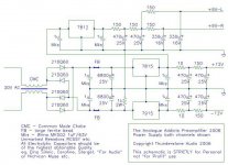
Analogue Addict Phono
Before I design my own I would like to start with the
phono pre-amp design in the following thread:
http://www.diyaudio.com/forums/anal...-addicts-phono-preamplifier-2006-edition.html
But I will replace the OPA 637 by OPA 627 or AD8620. In
case AD8620 I would like to use the other half as
subsonic filter. I have both OPA and AD with me. I will
make it for MM type cartridge only. That will make the
whole thing simple including power supply.
Suggestions or encouragements are looked for as always.
Regards
Roushon
Attachments
AN-1651
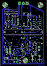
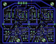
I am also working on the AN-1651 active/passive design.
1. Changed the gain of the first stage down to 30dB
as suggested in the notes to make it suitable for
MM type cartridge.
2. The pcb is redone completely to meet some of the
important points raised by Calvin.
3. The coupling pair of caps for each ic will be on the
track side directly soldered. Some provisions have
been kept by extending the GND.
4. There is a separate GND extended from the
main GND input for the preamp stage, may be not
necessary.
5. Track length to the ic pins have been considerably
shortened.
6. Loops on the power lines have be straightened.
There are now more jumper wires for this.
7. Will place a aluminium (or copper clad board) sheet
on the middle to separate the PS and the preamp stage.
8. The parts are the same as I have all of them.
9. Smaller caps choice will be implemented if found
suitable here.
Most likely overdoing again. Please let me know if there is any terrible mistake still.
Thanks
Roushon.
Attachments
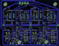
i have not proofed it, but i like you pcb
i am planning on trying the AN circuit p2p
Thanks! I think it is best to do a p2p at first. But I
am not good at it. Also making the pcb in home is easier
for me.
Roushon.
Matching capacitance...
I almost finished soldering the pre-amp board on my
homemade PCB as in the previous post with some little
modification on the PCB (separated the power input for
the two channels). Also got a new Project Debut III
turntable with Ortofon OM 5E cartridge.
Checked the capacitance with a digitial capacitance meter
at the end of the cable in the turntable. It reads 430pF
and 425pF. In the specification of the cartridge it says
recommended load capacitance is 200-600pF
The active/passive design in the AN-1651 aplication notes
(which I am making) has a 10pF at the input.
I would be thankful to know if the 10pF is enough or
I have to solder some more. I do not understand
this capacitance matching clearly.
Looking forward very much to a reply.
Best regards
Roushon.
Last edited:
- Status
- This old topic is closed. If you want to reopen this topic, contact a moderator using the "Report Post" button.
- Home
- Source & Line
- Analogue Source
- Phono-pre-amp+power supply pcb