_________________________________
Update: Revision 1 (Feb 23 2023)
After some further experiments HF distortion performance has been much improved from the first version previously posted. Decreasing R19/R20 to 470R (within safe margin to prevent parasitic oscillation) caused HF distortion to go down from about -80dB to -90dB, in both 50Watt/5R and 100W/5R tests. This modification puts usable feedback to work in a semi-local loop between the output stage and the VAS, in a more optimized way than before. The 10KHz spectrum shots have been updated with the new test results below.
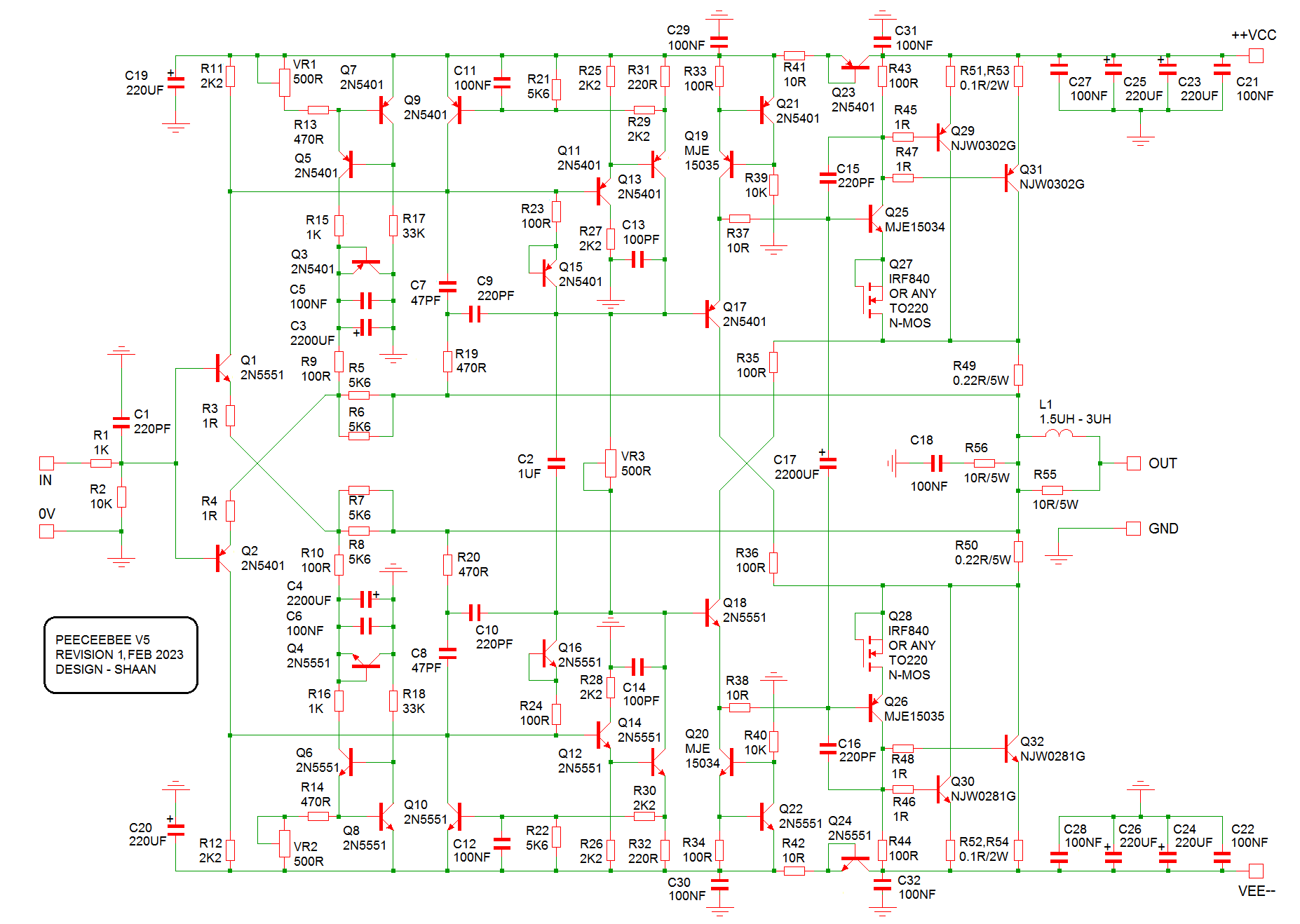
In the board silkscreen a few things have been changed thanks to Gary's input. Component markings have been improved and now it should be easier to read the numbering. Also a few components were missing in the schematic (that were present in the layout). This has also been corrected.
The pre-driver transistors Q17/Q18 have been oriented correctly to put their flat face in parallel with the drivers Q25/Q26 so that they can be properly thermally coupled with the driver transistors using zip ties. This thermal coupling ensures output bias stability.
Some texts added.
BOM and Setup guide has been uploaded. Please check the attachments section below.
_________________________________
Hello everyone.
Here is the latest version of PeeCeeBee, the V5. PCBs will be available through group buys in this thread. For the questions/discussion thread please follow this link >here<.
I have been on it since early 2022, and after a long series of experiments and listening tests the design was finalized in October end. The concept-build was done in early January and after some tweaks the amp took its current shape in late January this year. By that time the prototype layout was also completed and subsequently I got a pair printed, and after carefully listening to the prototype build for some time I felt that sound-wise the PeeCeeBee has moved one more step forward and it was time to release it.
This time we let the Lateral MOSFETs go and adopt the mighty Vertical MOSFETs, then vertically invert them and short them gate to source, then let them pass only a few tens of milliamps! The output devices are bipolar transistors. Why let the Laterals go? Well, I can't get genuine ones anywhere except Profusion PLC (Exicon). After the market basically went empty of Laterals following the pandemic, I realized I need to move on. But move where? Verticals are very nice devices when very hot, but not so nice at room temp. Meanwhile many audio friends suggested that I should go bipolar, and I thought "ok let's go bipolar". But after listening to the first bipolar-output peeceebee concept in June last year, I wasn't impressed to say the least. But bipolars are room-temperature-happy devices and many options are available from many manufacturers. This was intriguing. So I thought let's see where this goes. Experiments began. And here we are.
Description:
The PeeCeeBee V5 is a bipolar input - bipolar output symmetrical current-feedback amplifier with 32 transistors per channel (yes). And it still sounds musical! Some of the transistors are connected in such a way that makes it look like they are turned off for-ever. Well, they are turned off in a way. But as a matter of fact you cannot close-off all the channels inside a transistor unless you short all their pins with each other. In this circuit some of them are base-emitter shorted, and inverted. This turns the BJTs into base-collector diodes and the MOSFETs into source-drain diodes with the same reverse voltage ratings as their rated Vce or Vds. I decided to use them as emulated diodes in order to get rid of the hassle of looking for suitable discrete diodes (and to scare the members who count transistors).
The small signal bipolar transistors have been changed from the previous BC546/556 pair to 2N5551/5401 pair. These are commonly available general-purpose transistors that have three times the voltage rating of the BC pair, but half the gain. The higher voltage rating was necessary, and we don't need high gain BJTs as we have many gain stages. Upto the VAS, the amplifier is almost the same as V4H, except the VAS current limiters have been modified with low-pass filters. The limiters now clamp VAS current to about 3.6mA DC, but allow the VAS transistors to source/sink higher currents at gradually higher frequencies. This eliminates the slew-rate limiting effect of the VAS current limiters, so the limiters can stay there after biasing and setup has been done and there is no longer any need to short any jumpers after the VAS current has been set. Looking at the output stage one might wonder why the limiters were made to source/sink higher current at higher frequencies when the output stage's pre-drivers Q17/Q18 have very high input impedance and only a few pF of capacitive load that the VAS needs to drive. Well, the charge/discharge current of the capacitors C7/C8/C9/C10/C13/C14 is sourced/sinked by VAS transistors Q13/Q14, and these capacitors add-up to a load of couple hundred pF for the VAS. If the VAS current limiters Q9/Q10 clamp VAS current at the same preset value for all frequencies then as we go to higher frequencies the amount of current needed for every charge/discharge cycle increases, but without the low-pass filters the limiters won't allow the VAS to deliver the higher current. The result is slew-rate limiting of the VAS, and subsequently the whole amplifier. With the low-pass filters present, the VAS current variatiations at high frequencies are made invisible to the limiters. The result is that VAS bias clamping at DC (to prevent overheating of the VAS transistors) remains effective while amplifier slew-rate remains intact.
The output stage is a "bootstrapped complementary-feedback-pair-diamond-triple buffer". A bit mouthful and yes it does have it's own quirks, but after some experiments it has grown to behave, and in the current design it works stably without any hiccup. The pre-driver emitters are constant current sourced to about 7mA, and their collectors are connected to the collectors of the power transistors of the opposite sides. This particular configuration of the diamond-buffer has the advantage that the pre-drivers have a very low voltage (both DC and AC of less than 3V at any output level including clipping) present between their collectors and emitters, i.e. they are bootstrapped, which nearly eliminates the non-linear effect of their Cob/Cbc a.k.a Early effect. The base-stoppers (R37/R38/R45/R46/R47/R48) are there to prevent localized oscillation at the output stage. As it turned out, despite the driver transistors having to drive the bases of two power transistors in parallel and in Sziklai config (which is comparatively less stable than pure Darlington config), the OPS is very stable with zero sign of parasitic/spurious oscillation.
Now let's talk about the two seemingly unnecessary vertical MOSFETS. The two MOSFETs are gate-source shorted and their parasitic source-drain diodes are utilized to give more room for the bias spreader pot and make output biasing easy. The MOSFETs could be eliminated and the OPS would still work. But then even with pre-driver bases shorted the quiescent bias is unpredictable and often hundreds of mA. One could use a simple diode in the place of the MOSFETs, but I find the idea of using the parasitic diodes interesting as long as it doesn't cause problem (it didn't). I am not fully sure whether the MOSFETs' parasitic diodes would add any sonic character of their own. As far as I can say from listening tests, if anythin is being added, it's of the good kind.
The drivers are MJE15034/15035 and output devices are NJW0281/0302 pair, chosen for their fantastic audio performance. Even with +/-50V rails, voltage across the pre-drivers remain so low at all output levels that you can safely use low voltage high gain bipolars here e.g. BC550C/560C. I have tested the amplifier with BC550C/560C and they work without any problem, but keep in mind that their pin configuration is C-B-E, while the 2N5551/5401 is E-B-C.
The two 1R resistors present at the emitters of the input transistors Q1 and Q2 are there just to make it easy to route the connections (the PCB design is 100% manually laid-out, no automation whatsoever). You may have noticed the input transistors are no longer closely placed, unlike all previous PeeCeeBees. This was done because the amplifier has excellent offset stability. Even with a temperature difference of 30C between Q1 and Q2 the offset varies less than 100mV. With the two input transistors spacing out from each other, some room in the middle of the layout was cleared for components that needed it.
The pre-drivers and drivers need to be thermally coupled using zip-ties for bias stability during temperature variation due to amplifier operation (check attached pictures). In my tests this thermal coupling performed well and kept output bias under control during high power tests and everything going through many hot-cold cycles. Because the output stage is CFP/Sziklai type, only the drivers need their temperature to be kept in check for a stable output bias. With 50V rails, small plate type heatsinks with 10mm x 20mm size and 2-3mm thickness should be fitted to the driver transistors Q25/Q26 (the heatsinks can be fitted without any insulator, if this is done then make absolutely sure that the small heatsinks don't touch anything else). No other transistors on the upper side of the board will need heatsinking. The CCS transistors Q19/Q20 will get warm, but their worst case dissipation is less than 500mW, and in normal usage it is near 300mW and fairly constant so they will not need heatsinks. The vertical MOSFETs Q27/Q28 dissipate less than 100mW so won't need heatsinking either.
In addition to the standard zobel, there is an onboard inductor+resistor network at the output to prevent oscillation in case a the load has a capacitive element present e.g. long speaker cables. The inductor L1 is made of enamelled copper wire of 1mm diameter, 18-21 turns on a 10mm former (an AAA battery can be used as a former). The turns can be overlapped/layered with 6-7 turns in each layer.
The 2200uF (C17) between the OPS drivers' bases is oversized. It could be as small as 10uF and the amp would still work fine. But I left it there because I thought the board looked cool with it.
_________________________________
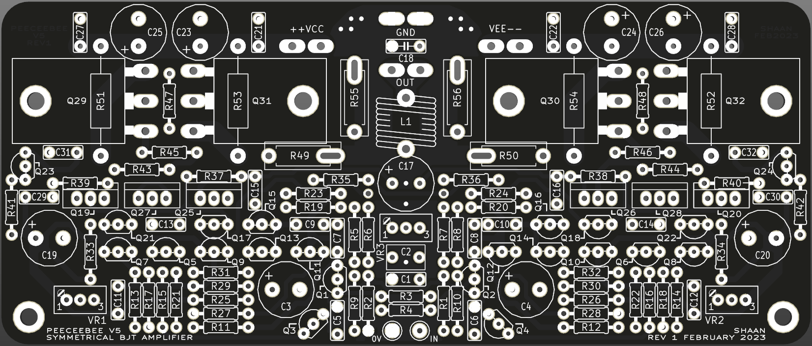
Here is the updated PCB snapshot:
Here is the updated schematic:
_________________________________
Subjective performance of the prototype:
How does it sound? Well, what I noticed is that it has tight bass, nice midrange and crystal clear highs, at just 10mA bias per output transistors, 20mA total o/p bias. Compared to the last version V4H, the midrange is not as forward, but relaxed and merged very well with the rest of the spectrum, but it's not weak either. I would say the midrange is very balanced. Vocals come out really well in my custom transmission line floorstanders made with the Alpair12P fullrangers. Cone control at bass is excellent, highs are pleasant as well. After testing many iterations over the months, I find that V5 in its current state sounds much better than V4H Revision 2 overall. And although it has many transistors, the amp is very musical, fatigue-free and does not sound clinical or harsh. With 15000uF reservoir per rail there is audibly zero hum or hiss present at the speaker.
_________________________________
Objective Performance:
Harmonic spectrum shots:
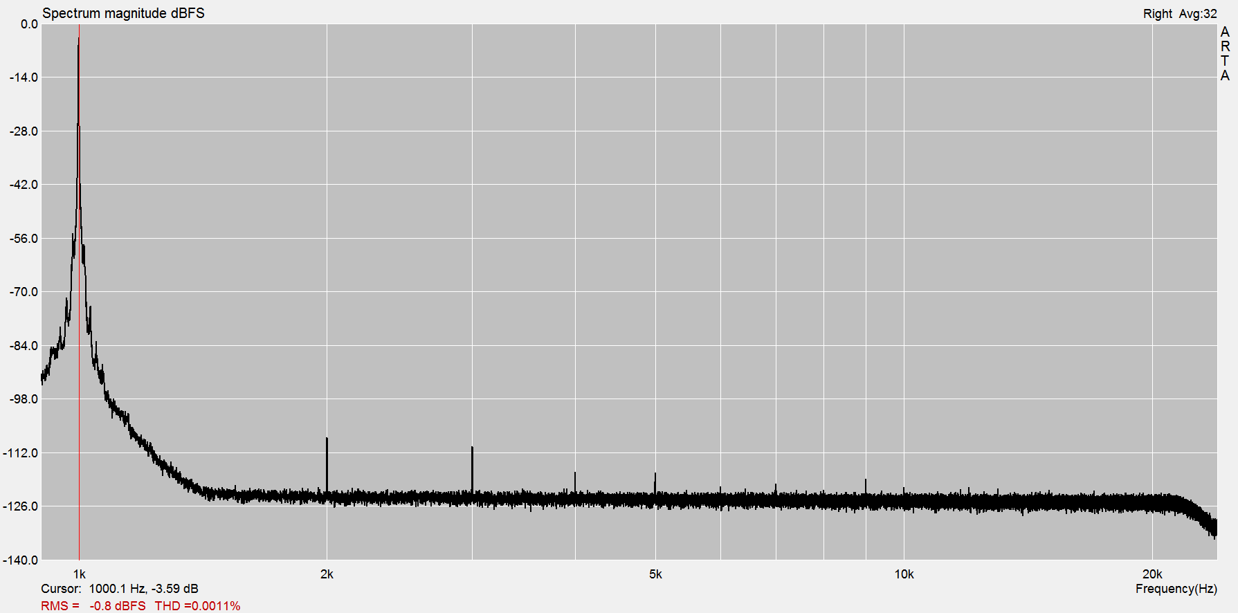
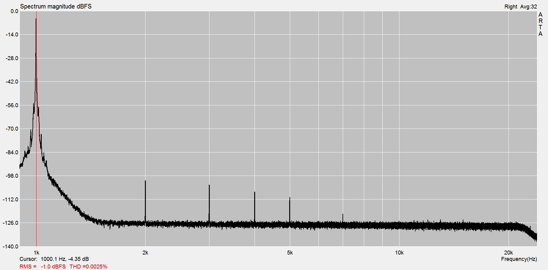
(1KHz - 0.001% source THD, 10KHz - 0.005% source THD, +/-50V rails, 2.5mA VAS bias, 200mA output bias, 5ohm resistive load)
1KHz 50W:
1KHz 100W:
1KHz 150W:
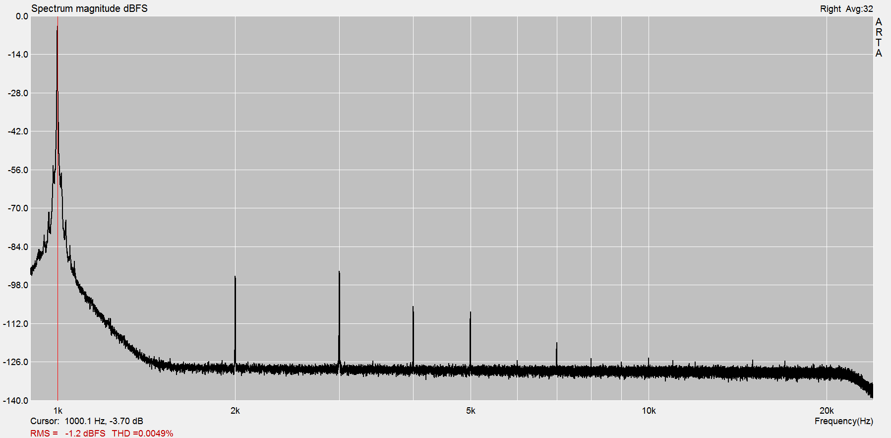
10KHz 50W:
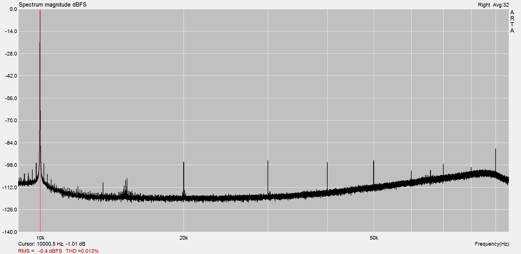
10KHz 100W:
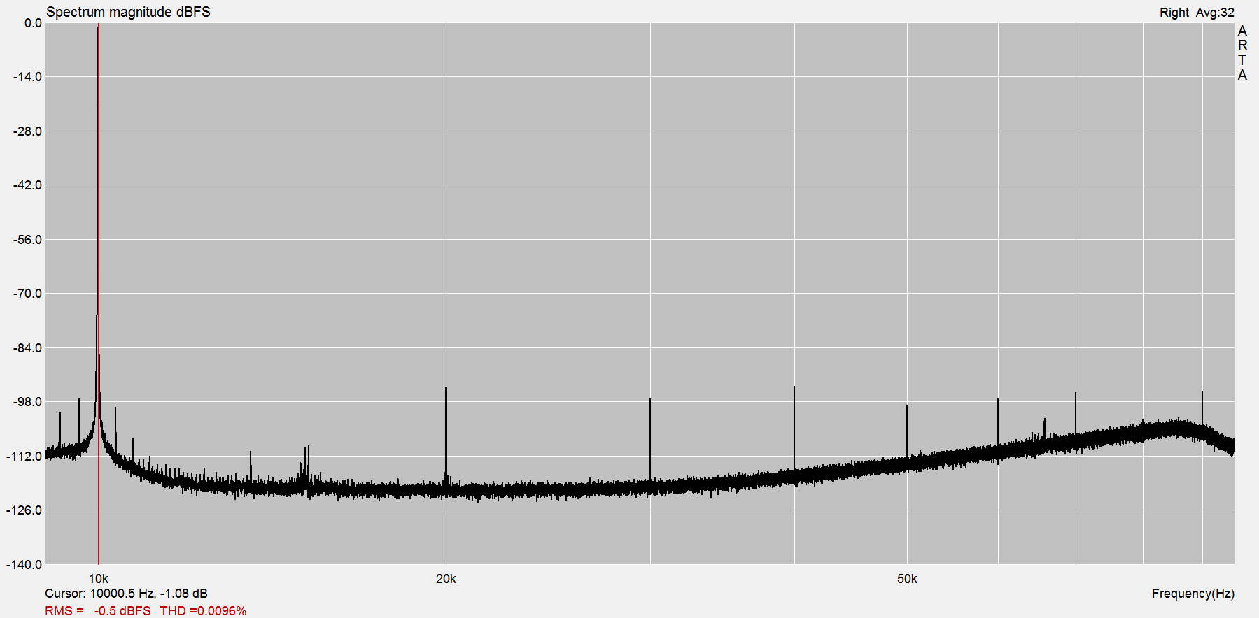
100KHz squarewave (asymmetrical duty cycle from signal generator):
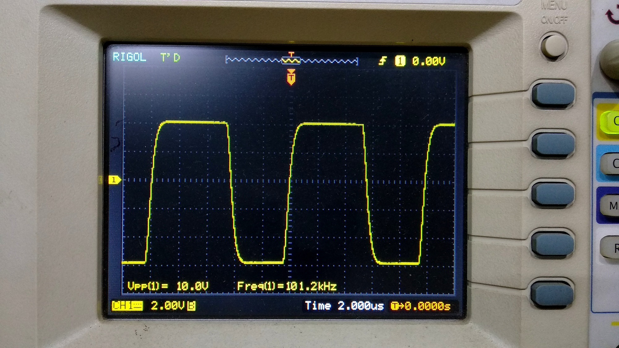
Capacitive load stability (5KHz squarewave into 2uF||10R, blue = before inductor, yellow = after inductor):
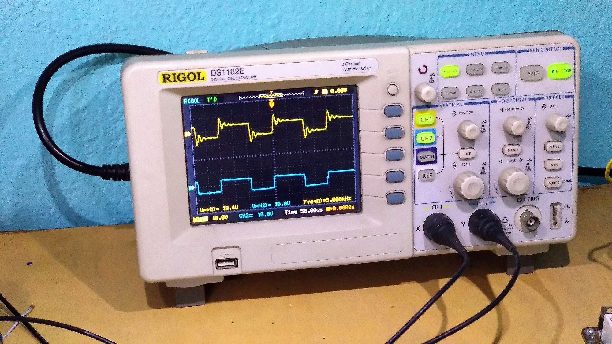
Slew rate:
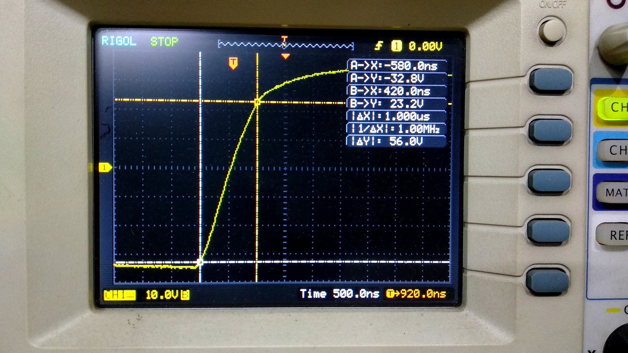
Second harmonic phase (1KHz fundamental):
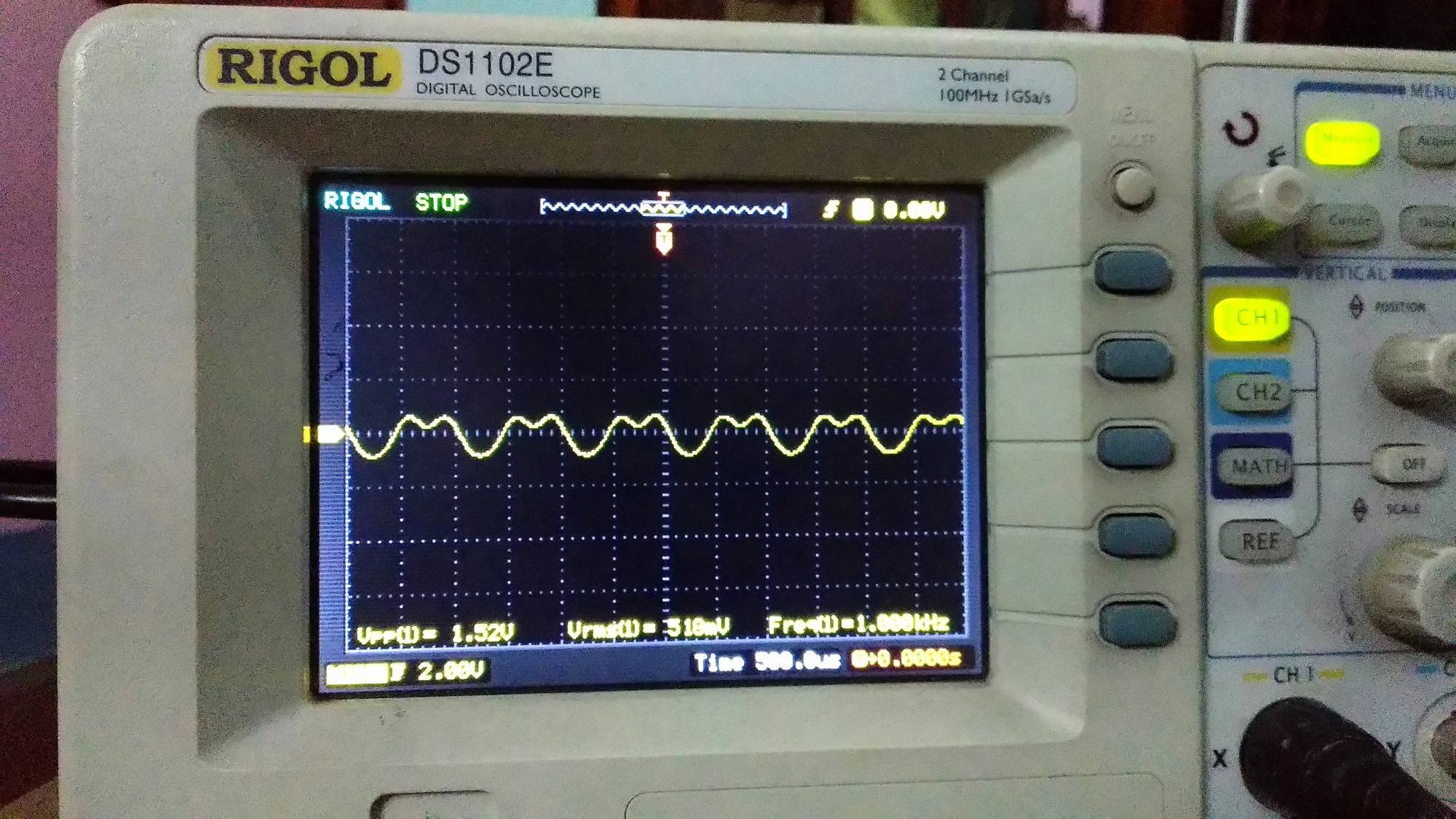
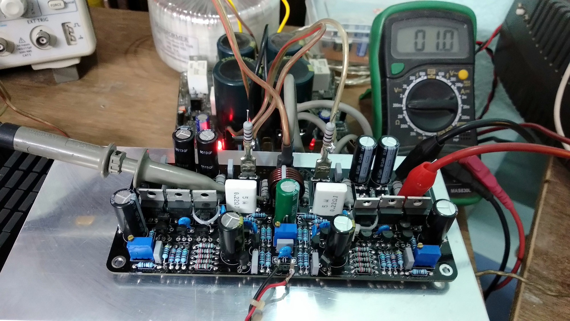
The prototype:
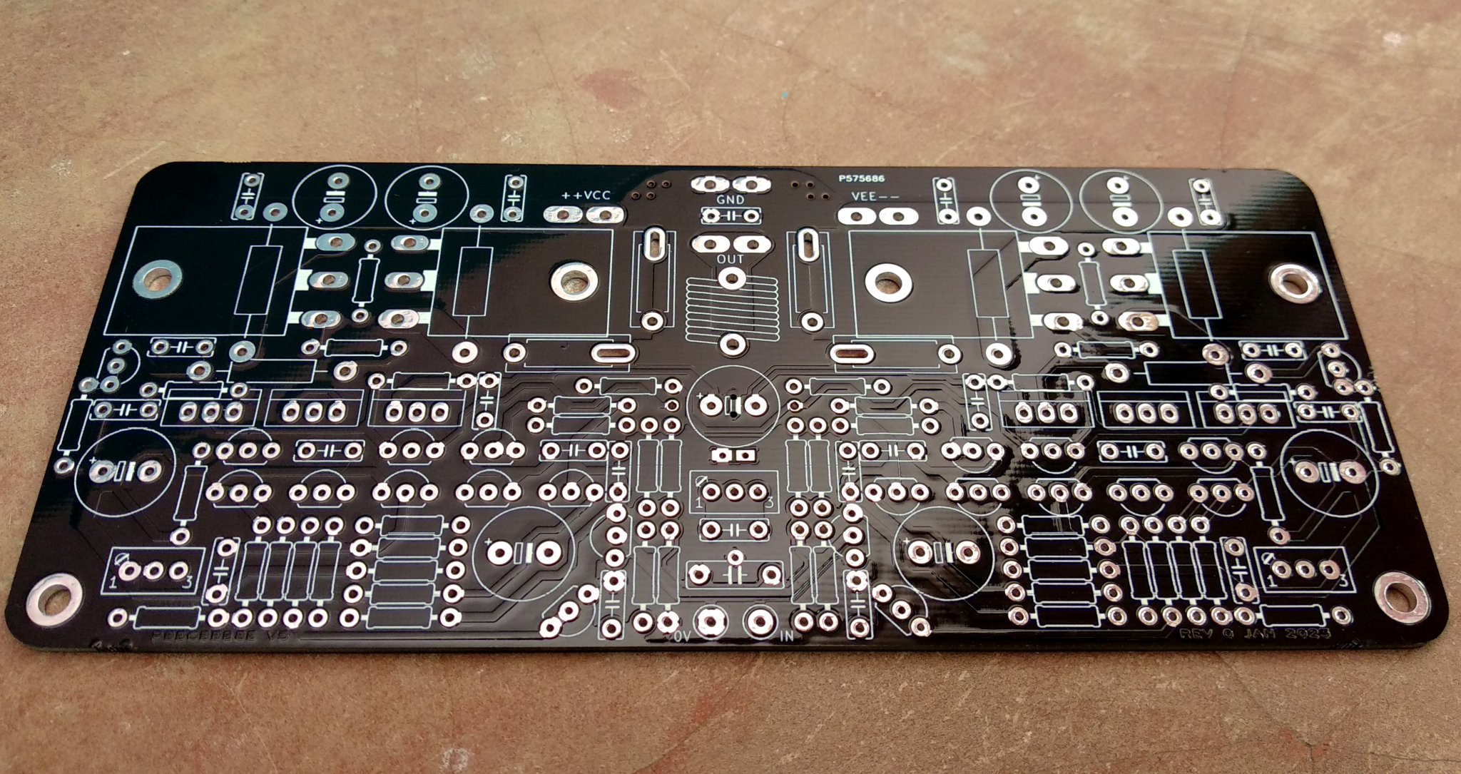
_________________________________
Specifications:
Power (+/-50V PSU, 0.1% THD) - 140Watt into 8R, 250Watt into 4R
Frequency response (simulated) - ~2Hz to ~700KHz (-3dB)
Slew Rate - 60V/uS
Offset variation - +/-10mV
SNR - 112dB+
AC gain - x28 (28.9dB)
DC gain - Unity
Input level for 250W into 4R - 1.2VRMS (~3.4V P-P)
_________________________________
BOM and Setup guide are being prepared and will be shared shortly.
_________________________________
GB info:
The PCB dimensions are 149.86mm x 63.5mm. PCB material FR4, PCB thickness 2.4mm, copper thickness 60 micron, 2 copper layers, black solder mask, white silkscreen, isolated mounting holes, HASL finish.
PCB price is 20USD for one unit. One PCB has one channel (mono).
Two forms of shipping is available. Preferred mode of shipping will be confirmed via PM.
1. Tracked International Air Parcel: Takes about two weeks to reach, ships to most countries, somewhat costly, variable cost for different countries, shipping cost will be shared during PM confirmation of GB entry.
2. Tracked Registered Post: Takes about four weeks to reach, ships to most countries, cost USD10 for all countries upto six PCBs in one consignment.
After GB entry PM will be sent to each member for email and shipping address. Invoices will be sent to each member and entry will be confirmed after payment for PCB + shipping cost. Please note that there is a 9% transaction charge for each paypal transaction; I always mention it separately in the invoice. Batch of 50 PCBs or more will be printed depending on interest. Time between placing batch order for the PCBs and getting the batch at hand is between 20 and 25 days.
_________________________________
Thank you and happy listening.
shaan
Update: Revision 1 (Feb 23 2023)
After some further experiments HF distortion performance has been much improved from the first version previously posted. Decreasing R19/R20 to 470R (within safe margin to prevent parasitic oscillation) caused HF distortion to go down from about -80dB to -90dB, in both 50Watt/5R and 100W/5R tests. This modification puts usable feedback to work in a semi-local loop between the output stage and the VAS, in a more optimized way than before. The 10KHz spectrum shots have been updated with the new test results below.
In the board silkscreen a few things have been changed thanks to Gary's input. Component markings have been improved and now it should be easier to read the numbering. Also a few components were missing in the schematic (that were present in the layout). This has also been corrected.
The pre-driver transistors Q17/Q18 have been oriented correctly to put their flat face in parallel with the drivers Q25/Q26 so that they can be properly thermally coupled with the driver transistors using zip ties. This thermal coupling ensures output bias stability.
Some texts added.
BOM and Setup guide has been uploaded. Please check the attachments section below.
_________________________________
Hello everyone.
Here is the latest version of PeeCeeBee, the V5. PCBs will be available through group buys in this thread. For the questions/discussion thread please follow this link >here<.
I have been on it since early 2022, and after a long series of experiments and listening tests the design was finalized in October end. The concept-build was done in early January and after some tweaks the amp took its current shape in late January this year. By that time the prototype layout was also completed and subsequently I got a pair printed, and after carefully listening to the prototype build for some time I felt that sound-wise the PeeCeeBee has moved one more step forward and it was time to release it.
This time we let the Lateral MOSFETs go and adopt the mighty Vertical MOSFETs, then vertically invert them and short them gate to source, then let them pass only a few tens of milliamps! The output devices are bipolar transistors. Why let the Laterals go? Well, I can't get genuine ones anywhere except Profusion PLC (Exicon). After the market basically went empty of Laterals following the pandemic, I realized I need to move on. But move where? Verticals are very nice devices when very hot, but not so nice at room temp. Meanwhile many audio friends suggested that I should go bipolar, and I thought "ok let's go bipolar". But after listening to the first bipolar-output peeceebee concept in June last year, I wasn't impressed to say the least. But bipolars are room-temperature-happy devices and many options are available from many manufacturers. This was intriguing. So I thought let's see where this goes. Experiments began. And here we are.
Description:
The PeeCeeBee V5 is a bipolar input - bipolar output symmetrical current-feedback amplifier with 32 transistors per channel (yes). And it still sounds musical! Some of the transistors are connected in such a way that makes it look like they are turned off for-ever. Well, they are turned off in a way. But as a matter of fact you cannot close-off all the channels inside a transistor unless you short all their pins with each other. In this circuit some of them are base-emitter shorted, and inverted. This turns the BJTs into base-collector diodes and the MOSFETs into source-drain diodes with the same reverse voltage ratings as their rated Vce or Vds. I decided to use them as emulated diodes in order to get rid of the hassle of looking for suitable discrete diodes (and to scare the members who count transistors).

The small signal bipolar transistors have been changed from the previous BC546/556 pair to 2N5551/5401 pair. These are commonly available general-purpose transistors that have three times the voltage rating of the BC pair, but half the gain. The higher voltage rating was necessary, and we don't need high gain BJTs as we have many gain stages. Upto the VAS, the amplifier is almost the same as V4H, except the VAS current limiters have been modified with low-pass filters. The limiters now clamp VAS current to about 3.6mA DC, but allow the VAS transistors to source/sink higher currents at gradually higher frequencies. This eliminates the slew-rate limiting effect of the VAS current limiters, so the limiters can stay there after biasing and setup has been done and there is no longer any need to short any jumpers after the VAS current has been set. Looking at the output stage one might wonder why the limiters were made to source/sink higher current at higher frequencies when the output stage's pre-drivers Q17/Q18 have very high input impedance and only a few pF of capacitive load that the VAS needs to drive. Well, the charge/discharge current of the capacitors C7/C8/C9/C10/C13/C14 is sourced/sinked by VAS transistors Q13/Q14, and these capacitors add-up to a load of couple hundred pF for the VAS. If the VAS current limiters Q9/Q10 clamp VAS current at the same preset value for all frequencies then as we go to higher frequencies the amount of current needed for every charge/discharge cycle increases, but without the low-pass filters the limiters won't allow the VAS to deliver the higher current. The result is slew-rate limiting of the VAS, and subsequently the whole amplifier. With the low-pass filters present, the VAS current variatiations at high frequencies are made invisible to the limiters. The result is that VAS bias clamping at DC (to prevent overheating of the VAS transistors) remains effective while amplifier slew-rate remains intact.
The output stage is a "bootstrapped complementary-feedback-pair-diamond-triple buffer". A bit mouthful and yes it does have it's own quirks, but after some experiments it has grown to behave, and in the current design it works stably without any hiccup. The pre-driver emitters are constant current sourced to about 7mA, and their collectors are connected to the collectors of the power transistors of the opposite sides. This particular configuration of the diamond-buffer has the advantage that the pre-drivers have a very low voltage (both DC and AC of less than 3V at any output level including clipping) present between their collectors and emitters, i.e. they are bootstrapped, which nearly eliminates the non-linear effect of their Cob/Cbc a.k.a Early effect. The base-stoppers (R37/R38/R45/R46/R47/R48) are there to prevent localized oscillation at the output stage. As it turned out, despite the driver transistors having to drive the bases of two power transistors in parallel and in Sziklai config (which is comparatively less stable than pure Darlington config), the OPS is very stable with zero sign of parasitic/spurious oscillation.
Now let's talk about the two seemingly unnecessary vertical MOSFETS. The two MOSFETs are gate-source shorted and their parasitic source-drain diodes are utilized to give more room for the bias spreader pot and make output biasing easy. The MOSFETs could be eliminated and the OPS would still work. But then even with pre-driver bases shorted the quiescent bias is unpredictable and often hundreds of mA. One could use a simple diode in the place of the MOSFETs, but I find the idea of using the parasitic diodes interesting as long as it doesn't cause problem (it didn't). I am not fully sure whether the MOSFETs' parasitic diodes would add any sonic character of their own. As far as I can say from listening tests, if anythin is being added, it's of the good kind.

The drivers are MJE15034/15035 and output devices are NJW0281/0302 pair, chosen for their fantastic audio performance. Even with +/-50V rails, voltage across the pre-drivers remain so low at all output levels that you can safely use low voltage high gain bipolars here e.g. BC550C/560C. I have tested the amplifier with BC550C/560C and they work without any problem, but keep in mind that their pin configuration is C-B-E, while the 2N5551/5401 is E-B-C.
The two 1R resistors present at the emitters of the input transistors Q1 and Q2 are there just to make it easy to route the connections (the PCB design is 100% manually laid-out, no automation whatsoever). You may have noticed the input transistors are no longer closely placed, unlike all previous PeeCeeBees. This was done because the amplifier has excellent offset stability. Even with a temperature difference of 30C between Q1 and Q2 the offset varies less than 100mV. With the two input transistors spacing out from each other, some room in the middle of the layout was cleared for components that needed it.
The pre-drivers and drivers need to be thermally coupled using zip-ties for bias stability during temperature variation due to amplifier operation (check attached pictures). In my tests this thermal coupling performed well and kept output bias under control during high power tests and everything going through many hot-cold cycles. Because the output stage is CFP/Sziklai type, only the drivers need their temperature to be kept in check for a stable output bias. With 50V rails, small plate type heatsinks with 10mm x 20mm size and 2-3mm thickness should be fitted to the driver transistors Q25/Q26 (the heatsinks can be fitted without any insulator, if this is done then make absolutely sure that the small heatsinks don't touch anything else). No other transistors on the upper side of the board will need heatsinking. The CCS transistors Q19/Q20 will get warm, but their worst case dissipation is less than 500mW, and in normal usage it is near 300mW and fairly constant so they will not need heatsinks. The vertical MOSFETs Q27/Q28 dissipate less than 100mW so won't need heatsinking either.
In addition to the standard zobel, there is an onboard inductor+resistor network at the output to prevent oscillation in case a the load has a capacitive element present e.g. long speaker cables. The inductor L1 is made of enamelled copper wire of 1mm diameter, 18-21 turns on a 10mm former (an AAA battery can be used as a former). The turns can be overlapped/layered with 6-7 turns in each layer.
The 2200uF (C17) between the OPS drivers' bases is oversized. It could be as small as 10uF and the amp would still work fine. But I left it there because I thought the board looked cool with it.

_________________________________
Here is the updated PCB snapshot:
Here is the updated schematic:
_________________________________
Subjective performance of the prototype:
How does it sound? Well, what I noticed is that it has tight bass, nice midrange and crystal clear highs, at just 10mA bias per output transistors, 20mA total o/p bias. Compared to the last version V4H, the midrange is not as forward, but relaxed and merged very well with the rest of the spectrum, but it's not weak either. I would say the midrange is very balanced. Vocals come out really well in my custom transmission line floorstanders made with the Alpair12P fullrangers. Cone control at bass is excellent, highs are pleasant as well. After testing many iterations over the months, I find that V5 in its current state sounds much better than V4H Revision 2 overall. And although it has many transistors, the amp is very musical, fatigue-free and does not sound clinical or harsh. With 15000uF reservoir per rail there is audibly zero hum or hiss present at the speaker.
_________________________________
Objective Performance:
Harmonic spectrum shots:
(1KHz - 0.001% source THD, 10KHz - 0.005% source THD, +/-50V rails, 2.5mA VAS bias, 200mA output bias, 5ohm resistive load)
1KHz 50W:
1KHz 100W:
1KHz 150W:
10KHz 50W:
10KHz 100W:
100KHz squarewave (asymmetrical duty cycle from signal generator):
Capacitive load stability (5KHz squarewave into 2uF||10R, blue = before inductor, yellow = after inductor):
Slew rate:
Second harmonic phase (1KHz fundamental):
The prototype:
_________________________________
Specifications:
Power (+/-50V PSU, 0.1% THD) - 140Watt into 8R, 250Watt into 4R
Frequency response (simulated) - ~2Hz to ~700KHz (-3dB)
Slew Rate - 60V/uS
Offset variation - +/-10mV
SNR - 112dB+
AC gain - x28 (28.9dB)
DC gain - Unity
Input level for 250W into 4R - 1.2VRMS (~3.4V P-P)
_________________________________
BOM and Setup guide are being prepared and will be shared shortly.
_________________________________
GB info:
The PCB dimensions are 149.86mm x 63.5mm. PCB material FR4, PCB thickness 2.4mm, copper thickness 60 micron, 2 copper layers, black solder mask, white silkscreen, isolated mounting holes, HASL finish.
PCB price is 20USD for one unit. One PCB has one channel (mono).
Two forms of shipping is available. Preferred mode of shipping will be confirmed via PM.
1. Tracked International Air Parcel: Takes about two weeks to reach, ships to most countries, somewhat costly, variable cost for different countries, shipping cost will be shared during PM confirmation of GB entry.
2. Tracked Registered Post: Takes about four weeks to reach, ships to most countries, cost USD10 for all countries upto six PCBs in one consignment.
After GB entry PM will be sent to each member for email and shipping address. Invoices will be sent to each member and entry will be confirmed after payment for PCB + shipping cost. Please note that there is a 9% transaction charge for each paypal transaction; I always mention it separately in the invoice. Batch of 50 PCBs or more will be printed depending on interest. Time between placing batch order for the PCBs and getting the batch at hand is between 20 and 25 days.
_________________________________
Thank you and happy listening.
shaan
Attachments
Last edited:
Great news Shaan!
Will you start a dedicated GB thread to keep the list organized and keep technical questions here?
Hi Vincent.Whoopsie!!
I see now that this already is the GB thread
Good point. I opened a thread for V5 tech questions/discussions >here<.
Thanks.
shaan
Shaan,
Can you clarify the amount of output stage bias? In the ‘Subjective performance…’ section you mention 20mA total output stage bias but in the objective section you mention 200mA.
As you develop the BOM and instruction guide:
I would suggest clarifying the locations of the various transistors in this circuit due to the sheer number! Even in the pcb snapshot pic above, I’ve had to double check with the schematic a few times along with looking at your fully built pictures in the other thread to make sure of their location(s). Perhaps color coding or using a different letter designation instead of ‘Q’ for some of the transistors. I imagine that this circuit will only be built by intermediate and advanced builders but this may minimize some debugging questions in the future. One has to be quite methodical and organized when building up this pcb. My $0.02.
Thanks!
Anand.
The standard output stage Class-AB bias for these transistors are in the zone of 30-70mA per transistor, 60-140mA total bias. After I increased the bias to ~20mA the crossover distortion nearly vanished from the scope trace. I wondered how it may do at this bias and started playing music, although there might still be some high order harmonic components present, but it did not impede the enjoyment. At higher bias harmonics beyond 4th are more effectively attenuated but I noticed not much to change after going 150mA+. There is no particular reason for 200mA. I just set it there and let the tests run.Can you clarify the amount of output stage bias? In the ‘Subjective performance…’ section you mention 20mA total output stage bias but in the objective section you mention 200mA.
Does this look better?I would suggest clarifying the locations of the various transistors in this circuit due to the sheer number! Even in the pcb snapshot pic above, I’ve had to double check with the schematic a few times along with looking at your fully built pictures in the other thread to make sure of their location(s). Perhaps color coding or using a different letter designation instead of ‘Q’ for some of the transistors. I imagine that this circuit will only be built by intermediate and advanced builders but this may minimize some debugging questions in the future. One has to be quite methodical and organized when building up this pcb. My $0.02.
Arrrgh, Agonizing, so many amps, so many DAC's, so many pre's, so many speakers, so much to learn, and so little time to build as we age . It's never about the money, always about the time. Will have to think about this one, as I need to build the V4H also. Shouldn't have to think to long
Sent from Mexico (winter get away).
MM
Sent from Mexico (winter get away).
MM
- Home
- Group Buys
- PEECEEBEE V5 GB
