AndrewT said:Hi,
caps become the biggest space/pin pitch problem when you start experimenting.
Try to make sure every capacitor location has at least two (useful) pin pitch options and leave adequate space for physically large caps. PP are always bigger than PES/PET.
I would prefer to see 0.1inch pitch connectors alongside/under the 0.2inch pitch terminals you have shown. Then you have a choice of how you make the on/off board terminations.
What do the regs need for caps around the pins?
I will work around the caps issue, I need some more space on the board. I will add the .1 connector choice as well. I stuck on .2 cause thats whats in my parts box for screw connectors.
The caps for the regs, I have sized for 47uf.
Nuuk said:Where is the 270R on that diagram?
I built my schematic with an adj resistor. However I am going to replace that with a fixed one. That will allow me some more space or the pp cap choices as well.
I also spent some time last night matching the J310's I have some exact pairs and a lot within 0.1 milliamps of each other. I Can get 6 matched to within .4 milliamps of each other. What constitutes a matched pair in peoples opinions?
I got a case made today for my measurement mic, I gues I have less than 45 mins to get it completed then I will work flat out on the design above.
Regards
B

What about this one?
I'll try this very soon. I've got the components.
There are some differences;
- 2u2 used as DC decoupling instead of 4u7.. Why? because I already have 2u2.. However the space is suitable for 4u7 also.
- 2SK170 used as J2 as Pedja said. But without R2, bias current increases 10mA. Then to keep it 6mA I put 20R source resistor to SK170..
- Added gate (1K) and input load (100K) resistors to J1...
- +/-30v will be used for LM3875... Because I've sold my wharfedale 9.6s.. Now I have only 9.1s and theyre 86dB. So I will need more power..
Thats all. If anybody request, then I can send the eagle files..
An externally hosted image should be here but it was not working when we last tested it.
I'll try this very soon. I've got the components.
There are some differences;
- 2u2 used as DC decoupling instead of 4u7.. Why? because I already have 2u2.. However the space is suitable for 4u7 also.
- 2SK170 used as J2 as Pedja said. But without R2, bias current increases 10mA. Then to keep it 6mA I put 20R source resistor to SK170..
- Added gate (1K) and input load (100K) resistors to J1...
- +/-30v will be used for LM3875... Because I've sold my wharfedale 9.6s.. Now I have only 9.1s and theyre 86dB. So I will need more power..
Thats all. If anybody request, then I can send the eagle files..
My latest PCB design.
Tidied up the component sizes, for the 1 uf I have designed for the sonicap Gen1
I have moved the cap to the underside of the board, but printing one sided board
Dimensions work out at 43.18x 29.21mm (1.7' x 1.15')
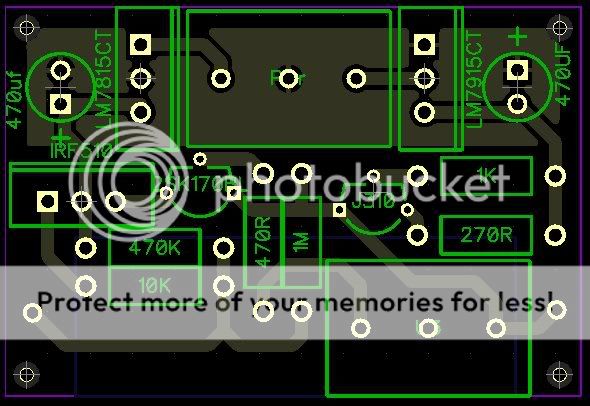
Whats the thoughts? Any errors or better design tips?
Had considered a signal earth plane?
Tidied up the component sizes, for the 1 uf I have designed for the sonicap Gen1
I have moved the cap to the underside of the board, but printing one sided board
Dimensions work out at 43.18x 29.21mm (1.7' x 1.15')
Whats the thoughts? Any errors or better design tips?
Had considered a signal earth plane?
Hello,
My compliments on your pcb design of the pedja buffer so far.
Yes, bypassing the regs close to the pins is a must.
You might want to reverse the position of the 470K and 10K resistors to position the 10K as close to the pin of IRF510 as possible.
By reversing the 470 ohm and 1M of position you can keep the traces for input and output as far away as possible from each other (basic rule in lay out).
You probably moved the 1uF to the underside of the pcb.
I have several formats of a 1uF capacitor like 32 x 11 or 26 x 8. Would these fit?
Do I notice right that you do not include the 4,7 uF capacitor nor the input filter of the LM3875 on the board. That is ok, but then they might hang around somewhere. For the bulky 4,7 uF this would not be a problem. The parts of the input filter might be worth to include.
When you order pcb's I might be interested in some.
Best, Arjen.
thanks Arjen, I am pleased that you like the board.
Good advice from you and Nordic as well. I will have a look at implementing the caps on the power pins as you suggest, I will also look at seperating the ground from the trace...
As for the filter, I had planned on impllementing this on another board.
The initial reason being so that the 4.7 cap could be something substantial, polyprops get kinda big at this value.
However I have just decided to take a step into Class D/T for the power output stages. I had bought 10 lm3886tf for outputs, but instead I am waiting for delivery of 5 ta2024 equiped boards from Sure for a punt.
these have a filter built in.
Later on I may or may not try again on the chipamp front.
Boards wise Arjen. i would be happy to do so... I am assuming that Pedja wont mind non-profit sharing.
Pedja is a legend, i emailed him today to ask him to have a look at it and he pointed out some stuff that i will have to check out. Mostly about pin orientations I will have a look at this tomorrow night and double check everything...
He referred me to a post I had looked at before, so I will have another scan over it and see if anything stands out...
And of course look at the caps for the power supply.
He referred me to a post I had looked at before, so I will have another scan over it and see if anything stands out...
And of course look at the caps for the power supply.
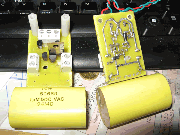
I've tested my combined PCB (Pedja buffer+LM3875) last evening.
http://www.diyaudio.com/forums/showthread.php?s=&threadid=124446
Its absolutely the best sounding chipamp I ever listened. Even with non-audio grade components (as you can see).
Strongly recommended!
An externally hosted image should be here but it was not working when we last tested it.
http://www.diyaudio.com/forums/showthread.php?s=&threadid=124446
Its absolutely the best sounding chipamp I ever listened. Even with non-audio grade components (as you can see).
Strongly recommended!
Dxvideo said:I've tested my combined PCB (Pedja buffer+LM3875) last evening.
Its absolutely the best sounding chipamp I ever listened. Even with non-audio grade components (as you can see).
Strongly recommended!
Finaly someone listened to me and made one...

Now add the regulated PSU I posted (also from Pedja), then you have top quality output from your GC...
regulated supply for the buffer alone or for the chipamp or for both?Nordic said:Now add the regulated PSU I posted (also from Pedja), then you have top quality output from your GC...
This is the PSU I made;
In the beginning it didnot work because of fake LM337. Not its ok and I dont hear any PSU noise.
I know that Pedja advices seperated PSU for the buffer however it works fine with this way also.
My buffer bias swings 5.95 - 6.05mA dependent on IRF510s temp. I think its normal..
PS: I am using 2SK170 +100R trimpot for the CCS.
PSII: The first stage of the psu is;
2 x 30v (independent secondary) 225VA toroid
2 x 35A metal case bridge rectifier
2 x 10,000uF/80v Nichicon
An externally hosted image should be here but it was not working when we last tested it.
In the beginning it didnot work because of fake LM337. Not its ok and I dont hear any PSU noise.
I know that Pedja advices seperated PSU for the buffer however it works fine with this way also.
My buffer bias swings 5.95 - 6.05mA dependent on IRF510s temp. I think its normal..
PS: I am using 2SK170 +100R trimpot for the CCS.
PSII: The first stage of the psu is;
2 x 30v (independent secondary) 225VA toroid
2 x 35A metal case bridge rectifier
2 x 10,000uF/80v Nichicon
- Status
- This old topic is closed. If you want to reopen this topic, contact a moderator using the "Report Post" button.
- Home
- Amplifiers
- Chip Amps
- Pedja Rogic Buffer and component choice for PCB design