The problem as fas as I understand is that with too large caps the "open window" of the rectifier becomes very short, making the current rise above the maximum of the rectifier (don't know how to properly say this in English). In this case, just substituting the rectifier bridge by one with a larger maximum current would solve the problem wouldn't it?
A question about the value of C12: the manual states that you can increase it if you like more bottom end. I'd like the roll-off to start a little later. Let's say keep it within -0.25dB at 30Hz, below 30Hz I don't mind roll off (probably even better to have it than not).
Which value to choose for C12? .22 in stead of .1?
Which value to choose for C12? .22 in stead of .1?
I have another question about the power supply:
the electrolytics are quite large. Is there a risk that I will blow the built-in fuse of the toroidal (thereby ruining it) when I switch the supply on? The charging electrolytics will cause a short power surge, is this too short to worry, or could it cause problems? The Pearl 2 itself adds another hefty amount of charging electrolytics by the way...
the electrolytics are quite large. Is there a risk that I will blow the built-in fuse of the toroidal (thereby ruining it) when I switch the supply on? The charging electrolytics will cause a short power surge, is this too short to worry, or could it cause problems? The Pearl 2 itself adds another hefty amount of charging electrolytics by the way...
matching 2SK170: how close is close enough?
I'm now measuring Idss of my first batch of 15 2SK170-BL (35 more on order in 2 batches). Range was 6,94-10,53mA. I have 4 pairs within 0,05mA. What should the maximum range between highest and lowest be in a pair or a quad to consider them "matched"?
I'm now measuring Idss of my first batch of 15 2SK170-BL (35 more on order in 2 batches). Range was 6,94-10,53mA. I have 4 pairs within 0,05mA. What should the maximum range between highest and lowest be in a pair or a quad to consider them "matched"?
NEED TROUBLESHOOTING HELP - Pearl 1
I've just finished a Pearl 1. Needs some help, not sure where to post...
It doesn't work, no 29 volts output from the on-board regulators (both channels- so whatever is wrong- whatever I did wrong- is the same on both boards)
This is my first Pass DIY, but I've built lots of DIY stuff before.
I've double-checked orientation of Q1, for sure it's OK. No short to the heatsink, either. Double checked all parts, all parts are in correctly, oriented right, etc. Measured all resistors, they are all as they should be.
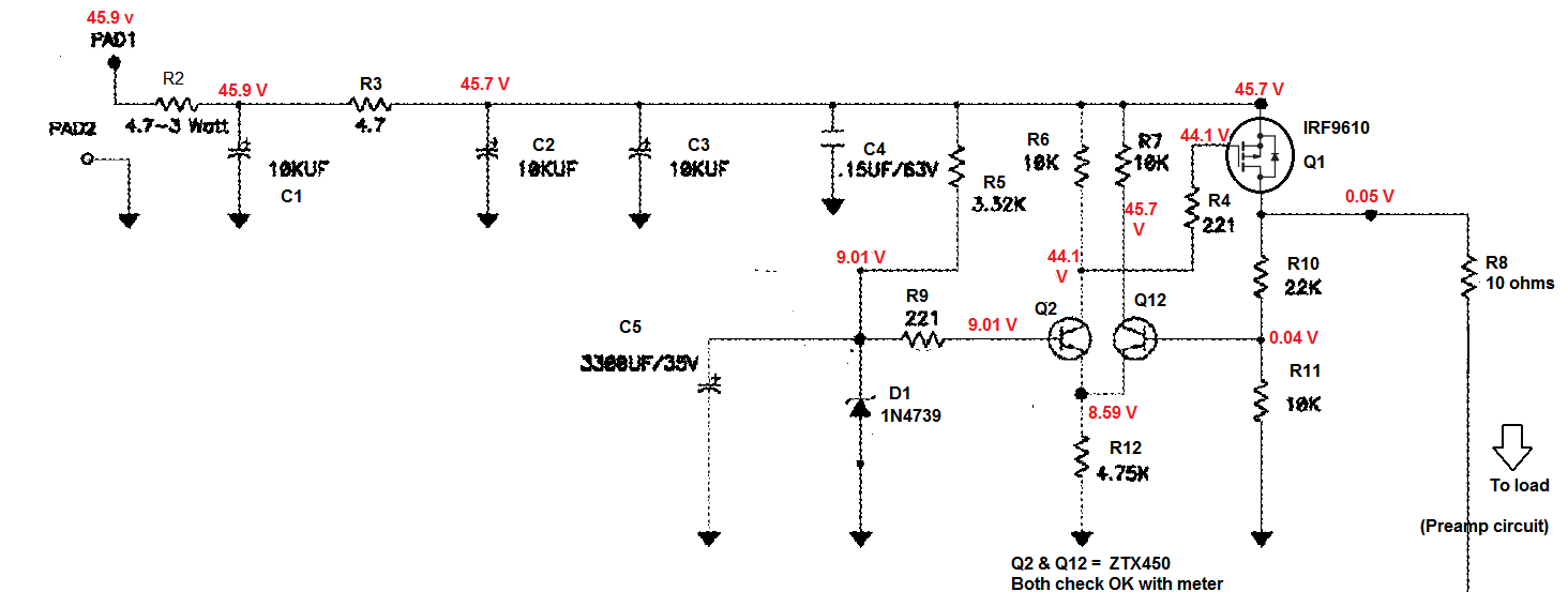
Here's some voltages:
DC INPUT (to R2) = 45.6 V
Q1
G 43.2 V
D 0.013 V same under no load (i.e., if R8 is removed)
S 45.1 V
Q2
E 8.44 V
B 8.97 V
C 42.1 V
Q12
E 8.44 V
B 0.013 V
C 44.0 V
D1 8.96 V
I guess I could shotgun it and replace Q1, Q2 and Q12.....
Any help is appreciated; or please point me to the correct forum and accept my apologies if I've mis-posted here.
I've just finished a Pearl 1. Needs some help, not sure where to post...
It doesn't work, no 29 volts output from the on-board regulators (both channels- so whatever is wrong- whatever I did wrong- is the same on both boards)
This is my first Pass DIY, but I've built lots of DIY stuff before.
I've double-checked orientation of Q1, for sure it's OK. No short to the heatsink, either. Double checked all parts, all parts are in correctly, oriented right, etc. Measured all resistors, they are all as they should be.
Here's some voltages:
DC INPUT (to R2) = 45.6 V
Q1
G 43.2 V
D 0.013 V same under no load (i.e., if R8 is removed)
S 45.1 V
Q2
E 8.44 V
B 8.97 V
C 42.1 V
Q12
E 8.44 V
B 0.013 V
C 44.0 V
D1 8.96 V
I guess I could shotgun it and replace Q1, Q2 and Q12.....
Any help is appreciated; or please point me to the correct forum and accept my apologies if I've mis-posted here.
Last edited:
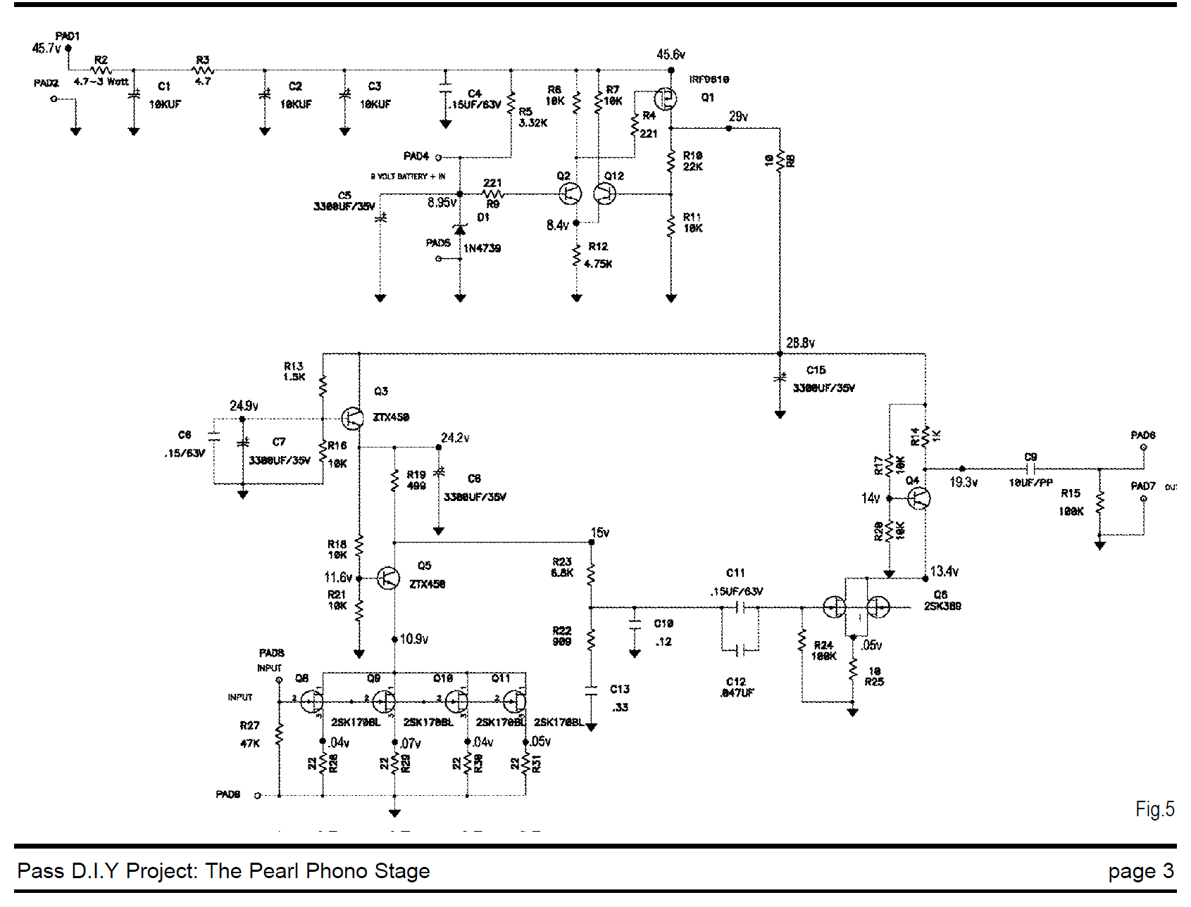
The Vgs on Q1 looks a little low. The voltage across R8 needs to be high enough to turn Q1 on. The voltage across R12 looks good. Check the value of R8?, is it 1K and not 10K?
BDP
R8 is specified to be 10 ohms in the schematic and parts list. I measure R8 to be 9.97 ohms.
I notice that the schematic (see above) shows the symbol for an N-channel MOSFET for Q1; it shows the part number as IRF9610, and the Parts List also shows Q1=IRF9610.
However, IRF9610 is a P-channel device... see http://www.vishay.com/docs/91080/91080.pdf
I think the circuit, as designed, would bias OFF a P-channel device. What goes on here?
Why does the schematic show an N channel MOSFET but the part number specified is P-Channel?
However, IRF9610 is a P-channel device... see http://www.vishay.com/docs/91080/91080.pdf
I think the circuit, as designed, would bias OFF a P-channel device. What goes on here?
Why does the schematic show an N channel MOSFET but the part number specified is P-Channel?
The schematic you posted shows 10K ohms and this would produce enough voltage to turn on Q1, which needs about 3 to 4 volts depending on the device.
Actually the schematic shows "10" for R8, and the Bill of Materials (parts list) shows "10 ohms" for R8
Not sure where you are seeing 10K for R8....
Do you mean R6? The "6" on the schematic does look kind of like an "8"
R6 is 10K ohms - I measure R6 to be 10,070 ohms.
Last edited:
Sorry, Yes, R6 the resistor in the collector of Q2. So if you only have 3 volts across R6,10K, that's .3 mA. Q12 is shut off. The current through R12 is 8.44v/4.75K = 1.77 mA. Where is the rest going? Whats the voltage across R4, if I have that one correct, gate resistor of Q1.
THANKS FOR HELPING ME WORK THROUGH THIS.
R4, 221 ohm resistor going to gate of Q1 has *NO* voltage drop across it, indicating NO current is flowing through the gate of Q1. I measured 43.3 volts on both sides of it. However, this is a MOSFET, so aside from charging up the gate capacitance and the Miller capacitance - which only takes about 20 nS - no current will flow through the gate. (well maybe a few picoamps) So, I don't think you'd expect any voltage drop across R4.
I'll measure more voltages tomorrow and post a schematic with voltages at just about every point on this voltage regulator circuit.
THANKS FOR HELPING ME WORK THROUGH THIS.
R4, 221 ohm resistor going to gate of Q1 has *NO* voltage drop across it, indicating NO current is flowing through the gate of Q1. I measured 43.3 volts on both sides of it. However, this is a MOSFET, so aside from charging up the gate capacitance and the Miller capacitance - which only takes about 20 nS - no current will flow through the gate. (well maybe a few picoamps) So, I don't think you'd expect any voltage drop across R4.
I'll measure more voltages tomorrow and post a schematic with voltages at just about every point on this voltage regulator circuit.
I've never built the Pearl I, but regulation works same as the one I currently use with the UGS (nearly finished). I'll try to help you
")
It works simple; Diode zener D1 is biased by a resistor, R5. This is the Vref of the diff. pair Q2/Q12. So you should first verify that the zener is correctly polarized, e.g. you got the good voltage across zener pins.
8,95V minus 45,6V gives a theoritical 36,65V drop on R5 3,32k, so a current of about 11 mA through this zener, which is a good value to start getting rid of zener noise
Chech for proper zener orientation if the current doesn't flow. You should have your Vdrop on R5, ideally Next, measure voltage drop on R12, 4K75. you should see something here, then calculate equivalent current flowing through the resistor and see if it's coherent with voltage drop across R6 and R7 (10k). On each half of the diff pair you should have 1/2 current of the one flowing through R12. If not, there is a trouble here, replace Q2 / Q12 and check good orientation of the bipolars pins. Collectors should be tied to the 10k resistors.
Ideally, seen the schematic you should have 8,4V across R12 4k75 i.e. 1,77 mA or so. And in each diff pair halves, 0,84 mA or so. Should give you voltage drop of about 8,42V or so per SE on the 10k resistors. Each collector should be at about 37,18V above ground.
This seems the value fed to gate of Q1, which is indeed a 9610, P_channel. Be careful to the pin orientation, output (regulated) is seen on the Drain, the Unreg V+ is fed to the Source pin of the mosfet. Gate value seems fairly high, as the mosfet would need about only 4-5V to start conducting, instead of the theoritical 8,42V we should find.
You should roughly find same voltage reading in the middle point between R19 / R11 ( 22k and 10k ) than the one you find on the zener ( 8,95v or so ). If not and every other readings are fine, then it's the 9610 that is either 180° reversed, or/and blown
I would also change the IRF9610 after having all precedent good values read.
It is the most sensitive device in the regulation, so if everyelse thing work, changing it in the end could achieve correct behaviour of the regulation
Hope you can start debugging the reg,
Best,
nAr
PS: To lower the noise floor of the PSU, R5 can be changed for a CCS (made of a jfet like K170GR, self biasing, IDSS chosen, 40V VDS limit or better K246GR/BL, 50V VDS limit) and the Zener by a LM336Z5 (or two in series), for example. Other resistor values may be adjusted to get good VOut values, like the ones in the bridge divider R19/R11.
Last edited:
THANKS!
Thanks! I had a vague idea about how this regulator works, but not a clear enough idea to predict what voltages I should see at various points.
I did guess that the problem might be the MOSFET Q1 itself, and so ordered four of them.
The Pearl that I am building was something I bought off an audio "FOR SALE" board, a fellow had bought the boards and all the parts a few years back but then had never built the thing. The MOSFETs have been laying in his back closet for a few years, and they were NOT in a conductive bag. The smaller FETs were wrapped in aluminum foil, but the power MOSFETs were just in a plastic bag, so it is possible they are dead.
2 more questions about matching 2sk170
1. do Q4 and Q5 have to be Idss matched as Q6-9 or Vgs?
2. Is it important to have pairs and quads in the same Idss range for the two channels? (and within one channel?)
I now have 27 2SK170's (23 more on the way) and have defined 1 quad (within 0,6%) and multiple pairs (to within 0,1%). But the lowest pair is 7.98-7.99mA, the highest 10.52-10.53mA. Would it be a problem to use one of those in the left channel and the other in the right?
I've never built the Pearl I, but regulation works same as the one I currently use with the UGS (nearly finished). I'll try to help you
It works simple; Diode zener D1 is biased by a resistor, R5. This is the Vref of the diff. pair Q2/Q12. So you should first verify that the zener is correctly polarized, e.g. you got the good voltage across zener pins.
8,95V minus 45,6V gives a theoritical 36,65V drop on R5 3,32k, so a current of about 11 mA through this zener, which is a good value to start getting rid of zener noise
Next, measure voltage drop on R12, 4K75. you should see something here, then calculate equivalent current flowing through the resistor and see if it's coherent with voltage drop across R6 and R7 (10k). On each half of the diff pair you should have 1/2 current of the one flowing through R12. If not, there is a trouble here, replace Q2 / Q12 and check good orientation of the bipolars pins. Collectors should be tied to the 10k resistors.
Ideally, seen the schematic you should have 8,4V across R12 4k75 i.e. 1,77 mA or so. And in each diff pair halves, 0,84 mA or so. Should give you voltage drop of about 8,42V or so per SE on the 10k resistors. Each collector should be at about 37,18V above ground.
This seems the value fed to gate of Q1, which is indeed a 9610, P_channel. Be careful to the pin orientation, output (regulated) is seen on the Drain, the Unreg V+ is fed to the Source pin of the mosfet. Gate value seems fairly high, as the mosfet would need about only 4-5V to start conducting, instead of the theoritical 8,42V we should find.
You should roughly find same voltage reading in the middle point between R19 / R11 ( 22k and 10k ) than the one you find on the zener ( 8,95v or so ). If not and every other readings are fine, then it's the 9610 that is either 180° reversed, or/and blown
I would also change the IRF9610 after having all precedent good values read.
It is the most sensitive device in the regulation, so if everyelse thing work, changing it in the end could achieve correct behaviour of the regulation
Hope you can start debugging the reg,
Best,
nAr
PS: To lower the noise floor of the PSU, R5 can be changed for a CCS (made of a jfet like K170GR, self biasing, IDSS chosen, 40V VDS limit or better K246GR/BL, 50V VDS limit) and the Zener by a LM336Z5 (or two in series), for example. Other resistor values may be adjusted to get good VOut values, like the ones in the bridge divider R19/R11.
Here are the voltages I've measured. It sure looks like the IRF9610 is bad. I have ordered some IRF9610. Thanks for all the help.
Last edited:
1. do Q4 and Q5 have to be Idss matched as Q6-9 or Vgs?
Yes, as they are part of a differential pair, they benefit from IDSS matching too
1°) Ideally, again, yes, because the quad whole current defines the gain of the 1st stage ... more IDSS, more gain2. Is it important to have pairs and quads in the same Idss range for the two channels? (and within one channel?)
2°) The IDSS of the diff pair doesn't have to be as high as the one we want in the quads, because quiescent current is lower. Even some 5 mA IDSS here should work fine I now have 27 2SK170's (23 more on the way) and have defined 1 quad (within 0,6%) and multiple pairs (to within 0,1%). But the lowest pair is 7.98-7.99mA, the highest 10.52-10.53mA. Would it be a problem to use one of those in the left channel and the other in the right?
I don't think so. Ideally, use 2 close IDSS quads for each channel, and 2 close IDSS pair for the differentials
Best,
nAr
Last edited:
Here are the voltages I've measured. It sure looks like the IRF9610 is bad. I have ordered some IRF9610. Thanks for all the help.
Seems all is good except the 9610
Good luck for the final step nAr
- Home
- Amplifiers
- Pass Labs
- Pearl Two