Because you'll have to solder 30+ different connections to the top, to the ground plane, etc. And if the whole thing is masked, it will be a pain to remove the lacker. Plus your board will look all scraped up and ugly. Masking is not good for this kind of an amplifier build. I vote no masking.
Can i get two sets of each board and speaker prot?
me too....
For members who want to place order for the boards,
please send your orders as instruction in Post # 6
I am having some progress in the top copper layer now but I am still stuck with the bottom copper layer. The gerber it exports cannot be read by my CAM350 and the program just hangs while reading the gerbers.
please send your orders as instruction in Post # 6
I am having some progress in the top copper layer now but I am still stuck with the bottom copper layer. The gerber it exports cannot be read by my CAM350 and the program just hangs while reading the gerbers.
ground plane for pcb
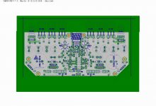
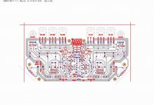
Here is the result of my weekend's work. Sorry it is in pdf format because my print-to-jpg software (Polestar Virtual Printer in case if you want to know or see how it works) is crazy. It sometimes give me the wrong color or some missing lines. Anyone can suggest a better software for that purpose? The grey area (not in your brain) is the top copper plane. Take a look at the 4 red squares.
There are still some problem with the bottem copper layer when exporting to gerbers. Hopefully I can solve that in 2 to 3 days time.
in Post#698, Godfrey talks about the long power ground path. I think I will take that off too (the red and the light green paths) so that every components would go to the power ground (it will be a ground plane after admendment) thru one of their leads and right at where they are located.
I am just wondering what I should do with the signal ground. If it is going to be the way I show in my attached pdf, it will be all (signal and power) connected together, not exactly like what was first intended.
Nagys,
You said you have to solder things onto the ground (power) plane. Just what exactly are those. Can you enlighten us with any photo. As far as I can understand, we are not soldering (or not necessary) things onto the plane itself, just the thrugh pad on the soldering side. Would you be talking about some additionals. Just want to know what is bothering you with a top soldering mask. It will be easy not to include the top soldering mask, it's just unusual to do so.
Attachments
bigpanda - Goldmund does not separate signal ground from power ground. As a matter of fact, every single ground point is soldered directly to the ground plane in the Goldmund amplifier, i.e. transistors, resistors, power supply from the bridge/transformer, negative terminal on the speaker output, negative terminal on the signal input, etc. Everything is soldered to the ground plane. Without the solder mask, it would make thing a lot easier, The ground tracks on the bottom of the circuit board are not even needed, but they are nice to have. It depends on how each individual builder wants to use the ground. I will probably only use the ground plane and nothing from the bottom of the circuit board.
Hi Nagys,
I will then take off both set of ground traces. Well, I feel less confined now.
All others
Here is the next problem list after the pcb :
1. The outputs
2. BSS71, 74
3. BC182
4. Panasonic relay -- I might have spotted at my supplier but lead time is 21 days and MOQ = 200pcs. But it is not exactly the one Alex drew, it is a TMP 1 Form A, slightly bigger (~1mm on each side) and rectangular. Leg pattern are the same but the position relative to the case is unknown.
5. L1
6. 4W resistors 0.7" pitch
7. 2W resistors 0.5" pitch
8. 4.7p
These are the components I would consider as 'trouble makers'
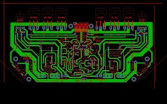
Still fighting with the bottom copper layer.
I will then take off both set of ground traces. Well, I feel less confined now.
All others
Here is the next problem list after the pcb :
1. The outputs
2. BSS71, 74
3. BC182
4. Panasonic relay -- I might have spotted at my supplier but lead time is 21 days and MOQ = 200pcs. But it is not exactly the one Alex drew, it is a TMP 1 Form A, slightly bigger (~1mm on each side) and rectangular. Leg pattern are the same but the position relative to the case is unknown.
5. L1
6. 4W resistors 0.7" pitch
7. 2W resistors 0.5" pitch
8. 4.7p
These are the components I would consider as 'trouble makers'
Still fighting with the bottom copper layer.
bigpanda - I would leave the ground traces on the bottom of the PCB. Everything can be soldered to these ground traces, the power and signal ground can be connected with jumpers, and the ground plane can also be connected to the power ground and signal ground. See, this way there are a lot of options, because each individual builder might want to build their amp differently.
If you do take the signal and power ground traces off of the bottom of the PCB, then the ground plane would have to be preferably modified slightly. All the ground places should have the metal going all the way to the components leg, so that it can be easily soldered from the top.
1.) Why is there a problem with the outputs? They're 100% fine the way they are. People should use the plastic type as the metal can original Hitachi 2SK134/2SJ49 are virtually impossible to find. The only thing that potential builders will have to change is the BIAS resistor R23 in Alex's schematic, 330ohm. This resistor will have to be changed to 220ohm, otherwise the MOSFETS might run slightly too hot. Here are all the current equivalent MOSFETS:
Renesas 2SK1058/2SJ162
Renesas 2SK1057/2SJ161
Renesas 2SK1056/2SJ162
Exicon ECX10N16/ECX10P16
Exicon ECX10N20/ECX10P20
Magnatec BUZ900P/BUZ905P
Magnatec BUZ901P/BUZ906P
Magnatec BUZ902P/BUZ907P
Magnatec BUZ903P/BUZ908P
2.) There's nothing you can really do with the Motorola BSS71/BSS74. There's really not an exact replacement available. You can get NOS on eBay and that's where I would suggest people get them from. They're also available from quite a few online electronic parts distributors. You can substitute them with MPSA92/MPSA42 with probably no modifications, but I can't guarantee it. If the originals are not used, then it's up to the individual builder to come up with a creative solution for a replacement and all the necessary changes to the schematic. Also, these transistors DO NOT need a heatsink. No reason for any heatsinks on them, they do not get hot.
3.) BC182B is available everywhere and should not be a problem at all.
4.) Relay replacement I'm still working on and will get back to you shortly.
5.) L1 is a 22 turn inductor. It can be wound in 2 layers around the resistor to make it smaller. I would make a 22 turn inductor, measure the mH, then wind it in 2 layers around the resistor and double check the mH. This shouldn't be a problem whatsoever.
6.) I don't see any problem here.
7.) I don't see any problem here.
8.) 4.7pF capacitors should be small ceramic types. I don't see any problem here either.
bigpanda - I thought about this would like to request that you please leave the signal ground, separate from the power ground, plus the ground plane just like in Alex's original PCB design. I think this is important because it's more flexible and will give more options to potential builders. Some people like the signal ground separated from the power ground, those who don't like it can connect it with jumpers. This way it makes everyone happy and gives lots of options when building this amplifier.
This is where you can buy the Motorola BSS71/BSS74 transistors:
Transistor BSS71 Motorola - eBay (item 170138825626 end time Oct-23-10 10:22:06 PDT)
BSS71 NPN, 200V, 0.5A, 40, 250, 10V, 0.03A, 50Hz, 500m - eBay (item 7507221065 end time Nov-09-10 13:15:50 PST)
BSS71 Transistor x 1 pieces - eBay (item 380277092960 end time Nov-07-10 08:50:54 PST)
BSS74 200V Vce, 0.5A Ic, 50MHz PNP bipolar transistor - eBay (item 3866832941 end time Nov-11-10 17:05:41 PST)
SEMELAB
KEYTRONICS STOCK SEARCH
BSS71 For buye?Technical Data?PDF?DataSheet - BSS71
BSS74 For buye?Technical Data?PDF?DataSheet - BSS74
BSS71, MOTOROLA - BSS71
BSS74, MOTOROLA - BSS74
And there's hundreds of other sources to get these transistors from. Not a rare part at all. Hope this helps everyone. Please use this original part in the schematic and you'll have no issues with building this amp.
BC182B is available from Newark/Farnell:
FAIRCHILD SEMICONDUCTOR|BC182B|TRANSISTOR, NPN, TO-92 | Newark.com
Plus hundreds of distributors online and sellers on eBay.
FAIRCHILD SEMICONDUCTOR|BC182B|TRANSISTOR, NPN, TO-92 | Newark.com
Plus hundreds of distributors online and sellers on eBay.
bigpanda - Sorry for so many posts. I would do the ground plane like in the .pdf you posted in post #24, in the red boxes. That's exactly how Goldmund does their ground plane. Even though this connects signal and power grounds together.
What do you think about also leaving the signal and power ground tracks on the bottom of the PCB board? I think we should leave them there, for more options. Builders who want to separate either power, or signal ground, can scrape off the little metal PCB tabs around the components holes. What are your thoughts?
As for the 2W R31, R38, R39, R35 and the 4W R32, R33... There's a little bit room there to maybe make thicker PCB traces.
R23 and R20 in Alex's schematic only need to be 1/4 watt. These resistors do not get hot and Goldmund uses 1/4 watt.
For resistors R31, R38, R39, R35, R32, R33, R36, and R37... I would recommend using Mills non inductive MRA-5 (5 watt) wirewound resistors. They're very small (only 0.5" in length) and easy to work with.
Last edited:
Nagys,
I would say top ground plane will be power ground (as I had done) and the signal ground remains as alex's design. 2 connectors at lower-mid board (as in alex's design also) which can be connected or seperately connected to outside. Not really necessary to keep the power ground trace. Should be able to finish them by to-morrow.
I have forgetten the most trouble maker -- 2N5565
I would still keep the power ground trace. Simply because of more options that can potentially make it easier to build. For example, I can easily solder all the resistors and transistors to the ground plane from the top, but what about capacitors, especially the big power supply capacitors? It might be difficult to solder those to the ground plane from the top. It can be easier to solder to the power ground trace first and then connect the power ground trace to the ground plane, if one choses to do that. I just think more options are better.
Also, can we leave the solder mask off from at least the ground plane?
As for the 2N5565, you can get them from many different places:
2N5565 Transistor x 1 pieces - eBay (item 380277086509 end time Nov-07-10 08:45:31 PST)
2N5565-E3 - price, delivery and datasheet for 2N5565-E3 - Planet One Components - Stocking Distributor
2n5565 2n5565 pdf 2n5565 datasheet 2n5565 Matched High Gain 16.0425 Transistors JFETs N-Channel Dual American Microsemiconductor 2n5565 available at 16.0425. FREE UPS ground shipping or more.
In-Stock 2N5565 - 4 Star Electronics 877-240-8595
Part: 2N5565 : AERI Electronic Components Distributor
2N5565 in stock - RfqHub.com - 2N5565 quotes comparing
2N5565 - NEW NSC NEW NSC 2N5565/NSC - Resellers Only!
Dale Electronics 1/Vishay Inventory by Distributor: Part 2N5565
I've got an idea, let's go one digit up :
2N5566
$7.20 each, $6.25/pc for +10 ?
Oh No, let's go one digit down then :
2N5564 => Radios For Sale
1 Dollah each, 6 for 5 buckeroos ?
Makes any sense ?
(didn't even have to check the Geekbay)
2N5566
$7.20 each, $6.25/pc for +10 ?
Oh No, let's go one digit down then :
2N5564 => Radios For Sale
1 Dollah each, 6 for 5 buckeroos ?
Makes any sense ?
(didn't even have to check the Geekbay)
Last edited:
Bigpanda - Here's what one of the members wrote and I completely agree with him.
"I've had just a quick look, the fuse on the PCB is ON FRONT of the big cap (4700uF) (not between C31 and C32) - on switch-on it could burn - unless a "slow" type used (?)"
This fuse should definitely be between C31 and C32 like in the schematic and it should be 10A. Can you please see if you can fix it. Thank you!
Bigpanda - After long consideration, I believe we should use this relay in the protection circuit: PANASONIC EW JTN1AS-PA-F-DC24V
It's a direct replacement for the original Panasonic relay that Goldmund used. This relay is in Panasonic's current production, is readily available everywhere, and costs around $4.
Please make sure that Alex's PCB for the protection circuit has the correct traces for this relay. Here are the specs: http://pewa.panasonic.com/assets/pcsd/catalog/jtn-catalog.pdf
- Home
- Group Buys
- PCB order for Goldmun clone