Just wondered if any of the PCB guru around had comments about this pcb. 
It's a simple headphones amp (opa2134+buf634t, I have some around). Actually only one layer, the red track is a thick wire running a few mm under the board. The rest is rather obvious. It will be standing right next to the regulator board, hence no electrolytics onboard. Thick traces and large tolerances for home etching.

Thanks in advance for any correction.
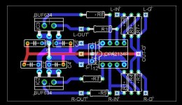
It's a simple headphones amp (opa2134+buf634t, I have some around). Actually only one layer, the red track is a thick wire running a few mm under the board. The rest is rather obvious. It will be standing right next to the regulator board, hence no electrolytics onboard. Thick traces and large tolerances for home etching.
Thanks in advance for any correction.
Attachments
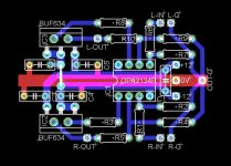
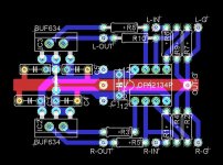
That looks reasonable for a single sided, etch your own layout.
You could move R3 closer to the OPA to make the signal path
shorter and further away from the output.
You could do the same with R10 on the other side.
Try and keep the in and out traces for the BUF634 as far apart
as practical.
You could move R3 closer to the OPA to make the signal path
shorter and further away from the output.
You could do the same with R10 on the other side.
Try and keep the in and out traces for the BUF634 as far apart
as practical.
To be honest ? Neither. I send the files to a guy ( etronics boutique réalisation de circuits ) who does simple pcb for cheap and does it well. It saves me time, I don't have to mess with etchant or drill plenty of holes and I don't have to buy supplies either.
Thanks for the comment btw
Thanks for the comment btw
- Status
- This old topic is closed. If you want to reopen this topic, contact a moderator using the "Report Post" button.
- Home
- Amplifiers
- Headphone Systems
- PCB check for a simple amp