I replaced the 6k8 with a 15k. That got me down to 1.2 volts with a 1.8 volt drop across the LED. Now I'm not getting any sound at all.
I havent plugged and played mine yet. I hope I don't get the same result.
Post #65 in this thread: http://www.diyaudio.com/forums/pass...no-phono-section.html?perpage=10&pagenumber=7 has some operational points that I checked mine against. I'm only getting .15v at the junction of q5 and q16 where I should be getting -27.6v according to that schematic. At the other end I'm getting 20v at Q17 and R52 where I should be getting -3.9v. I must have done something seriously wrong... maybe I need to try a different LED. I'm still getting 1.3v across R53 and R67 though.
Last edited:
So I had a few minutes to have a quick look -
Shouldn't matter at all, it means just the common sourced IRFP9610 is running at 30% more current (8.6mA instead of 6.6mA). I guess you have a LED with about 1.9V (the 1.6V LEDs in the XOno are pretty non-existent nowadays).
+0.15V sounds pretty ok for me; means the gate-source voltage of Q5 (input jfet half) is about this voltage negative as it should be.
I don't know where you got the -27.6 V from (I couldn't find anything from your link), but that would mean the constant current source has not any reasonable collector-emitter voltage to work with and that's certainly not intended.
You should get at this point a voltage of about -3 to -5 V (depending on output offset) as that's needed to run the push pull mosfets (about the same voltage, this time positive, for Q6/R26).
You can affect this value by changing the pot R25 and turn it to lower values (in original schematic that would be towards the upper end).
If that's the fault, you should measure much more than 0.35V across R28 or R27. If so, turn pot until you get these values.
Anyway, I'm sorry, with this little information I cannot help you much further.
If you find the time, it would make things a lot easier, if you could take a schematic and measure all voltages around Q1, Q16, output offset at R28/C7, Q3, Q6, Q7, Q18 and enter them into the schematic. All voltages with reference to ground and with the red probe")
That only cuts the current through the LED in about half, LED voltage drop changes only slightly. Does not sound like that's your problem. Unless it's not above wrong biasing, it's more likely that it's a wrong polarity fet or wrong connection or similar.
Don't give up ;-)
Hannes
All the values look good (other than getting 1.3v across R53)
Shouldn't matter at all, it means just the common sourced IRFP9610 is running at 30% more current (8.6mA instead of 6.6mA). I guess you have a LED with about 1.9V (the 1.6V LEDs in the XOno are pretty non-existent nowadays).
I'm only getting .15v at the junction of q5 and q16 where I should be getting -27.6v according to that schematic.
+0.15V sounds pretty ok for me; means the gate-source voltage of Q5 (input jfet half) is about this voltage negative as it should be.
I don't know where you got the -27.6 V from (I couldn't find anything from your link), but that would mean the constant current source has not any reasonable collector-emitter voltage to work with and that's certainly not intended.
I'm getting 20v at Q17 and R52 where I should be getting -3.9v.
You should get at this point a voltage of about -3 to -5 V (depending on output offset) as that's needed to run the push pull mosfets (about the same voltage, this time positive, for Q6/R26).
You can affect this value by changing the pot R25 and turn it to lower values (in original schematic that would be towards the upper end).
If that's the fault, you should measure much more than 0.35V across R28 or R27. If so, turn pot until you get these values.
Anyway, I'm sorry, with this little information I cannot help you much further.
If you find the time, it would make things a lot easier, if you could take a schematic and measure all voltages around Q1, Q16, output offset at R28/C7, Q3, Q6, Q7, Q18 and enter them into the schematic. All voltages with reference to ground and with the red probe
I replaced the 6k8 with a 15k.
That only cuts the current through the LED in about half, LED voltage drop changes only slightly. Does not sound like that's your problem. Unless it's not above wrong biasing, it's more likely that it's a wrong polarity fet or wrong connection or similar.
Don't give up ;-)
Hannes
Last edited:
I appreciate the help! I'm getting .344v across r27 and r28. I'm currently comparing my working channel against my broken one. So far the largest discrepency I've found is Q3.
Bad channel:
G:27v
D:27v
S: 24v
Good channel:
G: 4v
D: 27v
S: .4v
Q18 is messed up too.
Bad channel:
S: 23.6v
G: 20v
D: -26.7v
Good channel:
S: 1v
G: -3.5v
D: -26.7v
I'll get the rest of the values you asked for asap. Thanks again
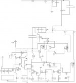
Edit: I traced the circuit out by hand and drew it up in Visio.
Bad channel:
G:27v
D:27v
S: 24v
Good channel:
G: 4v
D: 27v
S: .4v
Q18 is messed up too.
Bad channel:
S: 23.6v
G: 20v
D: -26.7v
Good channel:
S: 1v
G: -3.5v
D: -26.7v
I'll get the rest of the values you asked for asap. Thanks again
Edit: I traced the circuit out by hand and drew it up in Visio.
Attachments
Last edited:
So let's see -
(in the following I assume 30V rails, depending on your exact rails voltages might be slightly different)
Good - the push pull mosfets are correctly biased then. Is that only for the good channel?
27V at Q3-gate sounds ok (~1mA trough R4 as it should be).
27V at Q3-drain is too small; check that you get about 20.6V at R23/R6; if you get that value, check/replace the cascode transistor Q6.
Actually all these values of the good channel do not make any sense; for example source of Q3 cannot be at +0.4V as it should be connected to +30V.
Sounds ok! (Your rails are only a little low, 26.7 V instead of 30V and it seems you have about 1.5V dc offset).
That's really strange, seems your biasing arrangement (Q17,Q6,Q3) is messed up. You need to investigate there first.
Hannes
(in the following I assume 30V rails, depending on your exact rails voltages might be slightly different)
I'm getting .344v across r27 and r28.
Good - the push pull mosfets are correctly biased then. Is that only for the good channel?
Q3.
Bad channel:
G:27v
D:27v
S: 24v
27V at Q3-gate sounds ok (~1mA trough R4 as it should be).
27V at Q3-drain is too small; check that you get about 20.6V at R23/R6; if you get that value, check/replace the cascode transistor Q6.
Did you really measure 4V at G3-gate? Sounds more like you measured across R4.Q3.
Good channel:
G: 4v
D: 27v
S: .4v
Actually all these values of the good channel do not make any sense; for example source of Q3 cannot be at +0.4V as it should be connected to +30V.
Q18.
Good channel:
S: 1v
G: -3.5v
D: -26.7v
Sounds ok! (Your rails are only a little low, 26.7 V instead of 30V and it seems you have about 1.5V dc offset).
Bad channel:
S: 23.6v
G: 20v
D: -26.7v
That's really strange, seems your biasing arrangement (Q17,Q6,Q3) is messed up. You need to investigate there first.
Hannes
Good - the push pull mosfets are correctly biased then. Is that only for the good channel?
Nope, that's the bad channel. Good channel is .356v. This is after about 5 minutes of warmup.
27V at Q3-gate sounds ok (~1mA trough R4 as it should be).
27V at Q3-drain is too small; check that you get about 20.6V at R23/R6; if you get that value, check/replace the cascode transistor Q6.
I'm getting 27v at the junction of r23 and r6 on the bad channel. 19.1v on the good channel. 10 volts across R4 on the bad channel, 3.3v on the good.
Sounds ok! (Your rails are only a little low, 26.7 V instead of 30V and it seems you have about 1.5V dc offset).
Yeah, I'm getting closer to 27v/-27v. I'm temporarily using an lm317 with 47/1k resistors to regulate the power until I finish a salas shunt regulator.
I'm getting 27v at the junction of r23 and r6 on the bad channel.
We're getting somewhere - there is no current through R6.
Either the ground connection of R23 is loose or R23 is open. With 27V at this position, the cascode Q6 does not work, leaving Q3 infunctional.
10 volts across R4 on the bad channel
All current goes through the left (input) half of Q5; but fix first above problem with the voltage divider.
Yeah, I'm getting closer to 27v/-27v.
Just as a note, the original schematic says +-30V and I personally would prefer to remove the regulators to get there, as there is little headroom left for the fets.
Hannes
I'm measuring a .7v drop across R6 and a 27.1 drop across r23. I double checked the grounding and it looks okay, so I'll pull the resistors out and make sure they're both operable
The SMPS supplies I'm using are 48v if I remove the lm317. I assumed that'd be too much. I could mess with the values of the resistors hanging off of the lm317, but it seems close enough to work. I don't intend to put this thing in my 'official' system until I replace the lm317 with the shunt regulator. I'm in no rush since a certain 5 year old decided to "play DJ" with my turntable and ripped the needle off, so I need to wait a week or two until the new cartridge I ordered arrives.
Just as a note, the original schematic says +-30V and I personally would prefer to remove the regulators to get there, as there is little headroom left for the fets.
The SMPS supplies I'm using are 48v if I remove the lm317. I assumed that'd be too much. I could mess with the values of the resistors hanging off of the lm317, but it seems close enough to work. I don't intend to put this thing in my 'official' system until I replace the lm317 with the shunt regulator. I'm in no rush since a certain 5 year old decided to "play DJ" with my turntable and ripped the needle off, so I need to wait a week or two until the new cartridge I ordered arrives.
I'm measuring a .7v drop across R6 and a 27.1 drop across r23.
Seems Q6 is conducting and the little drop across R6 you see here is due to the 0.07mA base current of Q6 which sounds reasonable if Q6 has a beta of 100 or so. That's a little low, are you using 2SA991 or something else?
Check R23!
I'm in no rush since a certain 5 year old decided to "play DJ"
Yeah such things just happen.
Hannes
It's definitely a BC560. I pulled R23 out of the circuit and it measures 22.1k. This is what I'm reading on Q6:
good channel
e: 19.9v
b: 19.2v
c: 4v
Bad channel
e: 27.9v
b: 27.2v
c: 27.8v
Also, I don't know if this is relevant, but when I first built this circuit I could hear the music very dimly if I turned the volume to full. Now I can't hear any music at all. Maybe I burnt something out
good channel
e: 19.9v
b: 19.2v
c: 4v
Bad channel
e: 27.9v
b: 27.2v
c: 27.8v
Also, I don't know if this is relevant, but when I first built this circuit I could hear the music very dimly if I turned the volume to full. Now I can't hear any music at all. Maybe I burnt something out
Last edited:
It's definitely a BC560
You are aware that the BC560 has a different pinout than the original 2SA991?
Good channel behaves exactly as it should be, bad channel not yet
The problem with the bad channel is that only half of the differential pair Q5 is conducting, so Q3 is fully turned on and likely pushes too much current through R25/R25P.
Did you followed one of my previous posts and checked in the meantime the pot R25P and wether it influences this?
Hannes
EDIT:
Maybe I burnt something out
Sure that can easily happen.
This is really weird... I reconnected the board to the PSU and forgot to connect ground to the chassis (which is connected to safety ground). I measured -2.7v at Q17 and R52 with the black multimeter probe connected to chassis ground, but I'm back to 20.7v if I measure it with the black probe the circuit's ground. At the junction of r23 and r6 I get -1.5v from chassis ground, 27 volts from circuit ground. I measured -6 volts between the circuit ground and the chassis ground.
Last edited:
I'm glad to hear that!
Only thing that is important is the current through R67 and R53, not the LED-voltage itself.
You can scale R67 and R53 such that you get the same current; for example if you have a 1.83V led, you will see about 1.2 V across R67 and R53; if you increase the value of these resistors accordingly by these 20% to 570R and 180R you're back at the original currents (original resistor values with original 1.7V LED).
Enjoy! Hannes
EDIT: by the way, how come the other channel is fine with the same higher voltage LED?
Last edited:
The LED on the good channel was dropping closer to 1.7v, the bad one was closer to 2v. I've replaced both LEDs with ones that drop 1.83v for symmetry's sake.
The "bad" channel sounds distorted and twice as loud as the good one, so there's still something wrong with it. I'll take some measurements this morning.
The "bad" channel sounds distorted and twice as loud as the good one, so there's still something wrong with it. I'll take some measurements this morning.
Check Q6 (it might be simpler just to replace it).
However I don't fully understand your readings, how is it possible to have proper 3.5V across R4 with 21V at the gate of Q5 (non input half)? With that voltage at its gate it should turn on fully and conduct all current from Q16/R67 leaving R4 dry.
Hannes
Well, if the chassis is floating you can have any voltage between signal ground and chassis. Always measure with reference to signal ground.
However I don't fully understand your readings, how is it possible to have proper 3.5V across R4 with 21V at the gate of Q5 (non input half)? With that voltage at its gate it should turn on fully and conduct all current from Q16/R67 leaving R4 dry.
Hannes
I measured -6 volts between the circuit ground and the chassis ground.
Well, if the chassis is floating you can have any voltage between signal ground and chassis. Always measure with reference to signal ground.
- Status
- This old topic is closed. If you want to reopen this topic, contact a moderator using the "Report Post" button.
- Home
- Amplifiers
- Pass Labs
- Pass ONO or XONO PCB???