Well Guys,
I tried all types of pcb etching ways i found on INTERNET, so much of money spent on it, Trying to get the perfect track , But none of them was successful.
Toner transfer method is useful but not successful always. getting right type of paper is difficult, Even if you do ,purchase lot of it for future use. Then the right quality of laser print, oh god these cyber cafes never use original cartridges and then ironing .
But the best way i found is by photo resist film. It is wonderful.
No breaking sweat over improper tracks. I have etched many pcbs using this method, Even hairline tracks can be had with this method.
All it takes is 30 minutes and you have your pcb ready,
can u pls tell aabout this methord in detail plz.... help me..... i waste so much money on this
Toner transfer method....
It is nice to see this thread alive. My effort of starting this
thread seems to be paying off.
For making excellent quality PCB using toner transfer
method please read post nos 29 and 56. These two
posts explain in detail the steps to make PCB by this
method as well as gave the address for sourcing the
particular paper (chromo paper). This is the only method
I am using for years to make PCB with finer tracks
(for SMD etc). For copper clad board you can
order online from Visha Electronics in Mumbai.
Roushon.
pcb etching Using Photo Resist
Give me one day , I will give all the details.
can u pls tell aabout this methord in detail plz.... help me..... i waste so much money on this
Give me one day , I will give all the details.
Give me one day , I will give all the details.
I am also eager to know photo resist method in detail and
how to source the raw material.
Rouhson
Make your Own PCB with Photo Resist Process.
I am sharing the procedure which is used professionally and which I am using successfully for My Pcbs.
Required Tools-
1. Bare Pcb.
2. Photoresist Film.
3. Laminator or Hot water process which I will Describe.
4. Laser prints of your Pcb Mirrored on butter paper. Exposed area of Film will stay and rest will be washed out.
5. Uv Box.
5. Washing Soda for Developing.
6. Hydrochloric Acid
7. Hydrogen Peroxide.
8. Acetone or Thinner.
Procedure-
1. Clean your Pcb with very fine Water paper or Scotch brite clean it in running water till its Shines .Do not touch cleaned part with fingers as it may become greasy.
2. Applying Photo Resist Cut Photo Resist film about 1 inch Bigger than your Pcb on all sides.
Photo resist film is made of 3 parts.Top and bottom layer of Thin Plastic / Mylar layer. Mid layer Photo resist Chemical.
Scrap top layer with sharp blade to loosen an edge of top layer. Remove top layer and align film with pcb and let it pass through lamination Machine.
Hot Water Process- Requirement
Clothes Iron and Hot water in Spray Bottle.
Heat your Pcb with Home iron on cotton mode. Keep a layer of paper between iron and pcb . Do not touch iron to Pcb directly as it may deposit dirt.
As soon as your Pcb is hot Sprinkle the Pcb as well as Photo Resist Film with Spray of Hot Water. then start Aligning your Film from one side while Continuously rubbing film from one end to another as if you are removing water as well as bubbles with your thumb or Rubber squeeze . I have this in Pdf with Illustrations , if you need I Will mail it.
3. Uv Box -
Make a Wooden box of size about 12"width x 12" Height x 10" Depth. Attach a transparent Glass of Box Internal Dimensions. Attach two Uv tubes at Bottom, Distance between tube and Glass Partition 8".
Attach laser print on your Pcb coated with Photo Resist Film.
Printed side should face the pcb. keep Print side down on Uv Box Glass. Put some weight on the pcb so it sticks properly and evenly to Pcb.
Expose for 4 Minutes. Now you will have a image of your print on Pcb. Let it cool down for 10 Minutes. After that remove top Thin Plastic Layer.
4. Developing-
Prepare a solution of 1 table Spoon of washing soda and 1 Liter of Luke warm water, Mix it thoroughly. Dip your pcb in the solution , your print on Pcb Will Darken,after 1 min lightly scrub your pcb Lightly with soft brush keeping pcb in the solution . After about 2 to 3 min Unexposed part of film will be wahed away leaving bare pcb exposed and , Exposed area will remain on Pcb. Clean your Pcb with Running water.
5. Etching-
Prepare a solution of 2 parts Hydrogen Peroxide and one part Hydrochloric Acid in a Shalow Plastic Tray. Hydrogen Peroxide will oxidize Exposed PCB and Acid will Eat it. Sway your Tray as not to Spill any of the solution. in 1 min all exposed copper will be removed leaving Area under photo Resist film which are your Pcb tracks. Check for Shorts if none Clean Under Running water.
Now your PCB is ready , Drill it, You can Leave the film on tracks if you want as it will protect pcb from Oxidization and act as Flux.
Enjoy.
Attachments
Servicing test instruments...
In case you need to get repaired any test instrument (like
multimeter) try the following:
SaiTek Services
10/2B, 1st Flr Ahmed Mansion
366 Lamington Road
Mumbai-7
Tel: 23802304, 66546639
Mob: 9321313639, 9821313639, 9322236396
Email: saitek_s@yahoo.com
Roushon.
In case you need to get repaired any test instrument (like
multimeter) try the following:
SaiTek Services
10/2B, 1st Flr Ahmed Mansion
366 Lamington Road
Mumbai-7
Tel: 23802304, 66546639
Mob: 9321313639, 9821313639, 9322236396
Email: saitek_s@yahoo.com
Roushon.
I am sharing the procedure which is used professionally and which I am using successfully for My Pcbs.
Required Tools-
1. Bare Pcb.
2. Photoresist Film.
3. Laminator or Hot water process which I will Describe.
4. Laser prints of your Pcb Mirrored on butter paper. Exposed area of Film will stay and rest will be washed out.
5. Uv Box.
5. Washing Soda for Developing.
6. Hydrochloric Acid
7. Hydrogen Peroxide.
8. Acetone or Thinner.
Procedure-
1. Clean your Pcb with very fine Water paper or Scotch brite clean it in running water till its Shines .Do not touch cleaned part with fingers as it may become greasy.
2. Applying Photo Resist Cut Photo Resist film about 1 inch Bigger than your Pcb on all sides.
Photo resist film is made of 3 parts.Top and bottom layer of Thin Plastic / Mylar layer. Mid layer Photo resist Chemical.
Scrap top layer with sharp blade to loosen an edge of top layer. Remove top layer and align film with pcb and let it pass through lamination Machine.
Hot Water Process- Requirement
Clothes Iron and Hot water in Spray Bottle.
Heat your Pcb with Home iron on cotton mode. Keep a layer of paper between iron and pcb . Do not touch iron to Pcb directly as it may deposit dirt.
As soon as your Pcb is hot Sprinkle the Pcb as well as Photo Resist Film with Spray of Hot Water. then start Aligning your Film from one side while Continuously rubbing film from one end to another as if you are removing water as well as bubbles with your thumb or Rubber squeeze . I have this in Pdf with Illustrations , if you need I Will mail it.
3. Uv Box -
Make a Wooden box of size about 12"width x 12" Height x 10" Depth. Attach a transparent Glass of Box Internal Dimensions. Attach two Uv tubes at Bottom, Distance between tube and Glass Partition 8".
Attach laser print on your Pcb coated with Photo Resist Film.
Printed side should face the pcb. keep Print side down on Uv Box Glass. Put some weight on the pcb so it sticks properly and evenly to Pcb.
Expose for 4 Minutes. Now you will have a image of your print on Pcb. Let it cool down for 10 Minutes. After that remove top Thin Plastic Layer.
4. Developing-
Prepare a solution of 1 table Spoon of washing soda and 1 Liter of Luke warm water, Mix it thoroughly. Dip your pcb in the solution , your print on Pcb Will Darken,after 1 min lightly scrub your pcb Lightly with soft brush keeping pcb in the solution . After about 2 to 3 min Unexposed part of film will be wahed away leaving bare pcb exposed and , Exposed area will remain on Pcb. Clean your Pcb with Running water.
5. Etching-
Prepare a solution of 2 parts Hydrogen Peroxide and one part Hydrochloric Acid in a Shalow Plastic Tray. Hydrogen Peroxide will oxidize Exposed PCB and Acid will Eat it. Sway your Tray as not to Spill any of the solution. in 1 min all exposed copper will be removed leaving Area under photo Resist film which are your Pcb tracks. Check for Shorts if none Clean Under Running water.
Now your PCB is ready , Drill it, You can Leave the film on tracks if you want as it will protect pcb from Oxidization and act as Flux.
Enjoy.
dear sir ,
can you send me in illustrated form i want to see this procedure,plz also send me details about photo resist film,what is its local name and where we get it thanks
thanking u your ever masood
Last edited:
dear viki 2869316,I am sharing the procedure which is used professionally and which I am using successfully for My Pcbs.
Required Tools-
1. Bare Pcb.
2. Photoresist Film.
3. Laminator or Hot water process which I will Describe.
4. Laser prints of your Pcb Mirrored on butter paper. Exposed area of Film will stay and rest will be washed out.
5. Uv Box.
5. Washing Soda for Developing.
6. Hydrochloric Acid
7. Hydrogen Peroxide.
8. Acetone or Thinner.
Procedure-
1. Clean your Pcb with very fine Water paper or Scotch brite clean it in running water till its Shines .Do not touch cleaned part with fingers as it may become greasy.
2. Applying Photo Resist Cut Photo Resist film about 1 inch Bigger than your Pcb on all sides.
Photo resist film is made of 3 parts.Top and bottom layer of Thin Plastic / Mylar layer. Mid layer Photo resist Chemical.
Scrap top layer with sharp blade to loosen an edge of top layer. Remove top layer and align film with pcb and let it pass through lamination Machine.
Hot Water Process- Requirement
Clothes Iron and Hot water in Spray Bottle.
Heat your Pcb with Home iron on cotton mode. Keep a layer of paper between iron and pcb . Do not touch iron to Pcb directly as it may deposit dirt.
As soon as your Pcb is hot Sprinkle the Pcb as well as Photo Resist Film with Spray of Hot Water. then start Aligning your Film from one side while Continuously rubbing film from one end to another as if you are removing water as well as bubbles with your thumb or Rubber squeeze . I have this in Pdf with Illustrations , if you need I Will mail it.
3. Uv Box -
Make a Wooden box of size about 12"width x 12" Height x 10" Depth. Attach a transparent Glass of Box Internal Dimensions. Attach two Uv tubes at Bottom, Distance between tube and Glass Partition 8".
Attach laser print on your Pcb coated with Photo Resist Film.
Printed side should face the pcb. keep Print side down on Uv Box Glass. Put some weight on the pcb so it sticks properly and evenly to Pcb.
Expose for 4 Minutes. Now you will have a image of your print on Pcb. Let it cool down for 10 Minutes. After that remove top Thin Plastic Layer.
4. Developing-
Prepare a solution of 1 table Spoon of washing soda and 1 Liter of Luke warm water, Mix it thoroughly. Dip your pcb in the solution , your print on Pcb Will Darken,after 1 min lightly scrub your pcb Lightly with soft brush keeping pcb in the solution . After about 2 to 3 min Unexposed part of film will be wahed away leaving bare pcb exposed and , Exposed area will remain on Pcb. Clean your Pcb with Running water.
5. Etching-
Prepare a solution of 2 parts Hydrogen Peroxide and one part Hydrochloric Acid in a Shalow Plastic Tray. Hydrogen Peroxide will oxidize Exposed PCB and Acid will Eat it. Sway your Tray as not to Spill any of the solution. in 1 min all exposed copper will be removed leaving Area under photo Resist film which are your Pcb tracks. Check for Shorts if none Clean Under Running water.
Now your PCB is ready , Drill it, You can Leave the film on tracks if you want as it will protect pcb from Oxidization and act as Flux.
Enjoy.
when i put negative image on washed /clean pcb .and exposed it by uv light there was not a single line/shade .to get image on pcb which type of
chemical is sprayed.plz send me illustrated or picture form by seeing i can do this work.thanking you your ever masood
Thanks Viki for the information. In fact I need to solder some SMD. I went to
the Lamington Road today, but shops were closed.
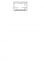
Toady got the address of the chromo paper dealer (attached is the scan). He
will send paper by post also. The rate is 500pieces A4 size Rs 220/-
+shipping. But I think it is best to purchase in person. The paper I have is
quite thin and that helps a lot.
Roushon.
dear roushan,
what is the other name of chromo paper in kanpur there is not available
in kanpur some screen printing material shop has technova paper which is transparent paper.is it right.thanksyours ever masood
For years I struggled to make my own PCB as like most of you. In a post
in this thread I gave the details of the chromo paper I finally found
in a shop in Flora Fountain area for toner transfer. Believe me I have
made at least 30 PCB of fine quality by this method. Two examples are
attached. Some of them are for SMD parts and most of them are double
sided. It takes only 20 minutes for a PCB if you uses hot ferric chloride
solution. This is to show and encourage you to another fruitful method.
One drawback as pointed out earlier about getting good laser print.
But in south Mumbai I got very good print out in a cyber cafe. May be
look around little bit more.
I promise to give you the address of the shop in Flora Fountain
in a few days. The chromo paper costs 400 sheets Rs 120/- only
two years back.
I hope you find it useful and saves your time...
N.B. Sorry, I do not have the picture of the pcb of the first board but it is
exactly as you see in the eagle design.
Roushon
dear roushan
before sticking/transferring film on fine pcb which type of chemical is sprayed on pcb to get fine/sharp picture .thanking you ur ever masood
dear roushan
before sticking/transferring film on fine pcb which type of chemical is sprayed on pcb to get fine/sharp picture .thanking you ur ever masood
Photoresist Film is laminated to the pcb before Exposing,Your image gets developed on this film. Dont use technova paper its is water soluble , will get washed away while Etching.
Photoresist Film is not available Locally, Only Pcb Makers Import them.
If you want Some, I can give you, Just pay Shipping and Packaging charges.
The method I Gave is quite easy to Understand.
dear viki v2
what amount will i pay thanks
masood
First 5 Feet i will Give free, pay 200rs for shipping and packing..
Give your complete address, and cell phone no.
First 5 Feet i will Give free, pay 200rs for shipping and packing..
Give your complete address, and cell phone no.
thank you i will pay rs.200 as advance by m.o.
thanks regard
Volume control pot
Hello to all,
I am looking for a sealed type dual volume control (100K), it
is better if it is motorized. Kindly tell me where can I find this in Mumbai.
I am sure it is available but to save some leg work it will be good if someone
gives an initial hint. After searching the net I found ALPS blue velvet are best but they
are phenomenally expensive, so most likely not available in India.
Thanks
Roushon.
Try Bhendi(chor) bazaar for old audio sets on the bazaar day. U might be lucky some day.
Gajanan Phadte
Thanks Gajanan! Although this suggestion always applies
for almost anything, it did not occur to me this time. I will
make a trip to that road sometime this week.
Roushon.
- Home
- Design & Build
- Parts
- Parts in Mumbai (India)