If the amplifier in question's a switchmode regulator or LDO it can be the difference between stability and instability, though usually one's just tuning the parts selection to maintain good phase margin (transient response) across the design corners. In the case of a signal amplifier you get (supply stuff)/PSRR on the output as discussed quite a bit over the last couple pages of this thread.What is the significance of phase angle or group delay, in a plot of the impedance seen by the amplifier power/gnd pins?
For analog audio I don't see a case in which supply phase considerations are signficant; reservoir caps turn inductive around 100kHz, sufficiently far above the audio band as to be irrelevant (assuming sufficient high frequency bypassing to keep the signal amp stable and off its slew rate). The same tends to hold for DACs. If you apply the -80dBish target I discussed a few posts back that means about a 10ns RMS jitter budget in 16/44.1. Low cost DACs come in around -100dB THD and, as I mentioned a few posts ago, it's not hard to build a supply which supports -110dB. That means that, among other things, if you don't want playback system performance to limit on the DAC you have a jitter budget in the range of 300ps to 1ns, halving for every clock doubling and extra bit. An ES9012 or ES9018 at 192kHz wants less than 20ps RMS to hit its -120dB THD and 3ps for its -135dB DNR in mono. Phase jitter from a decent XO with standard MLCC bypassing is around 3ps over 10kHz-20MHz, increasing a couple hundred fs if the integral's taken down to 10Hz. So, from the standpoint of an asynchronous DAC with a dedicated XO, the supply's essentially a non-problem and one's better off paying attention to impedance control and termination on the clock line to minizmise ISI.
More complex clock topologies create more complicated requirements. The limiting factor in generation is more often the supply than the clock itself. See, for example, table 1 in this thesis (page 26) as well as the design collateral for National/TI's LMK and LMX parts and TI's higher end CDCE parts. The femtosecond clock generators all use on die bypassing, on die regulation, and split external supplies and bypassing to improve performance. While overkill for audio there's a two or three order of magnitude performance gap between these and the low cost clock generators which come in at 100+ps (TI CDCE90x, for example). The low cost generators use similar split supply topologies but seem to lack the on die regulation of the higher cost parts. This implies one could perhaps get better performance out of the parts by devoting more cost to the external supplies. For example, the CDCE906 datasheet shows a phase noise hump between 2kHz and 500kHz which I suspect could be mitigated with a good local regulator with a large output bypass---perhaps a LM1117 followed by a Nichicon L8, S8, or R7. This is perhaps a bit quirky, but the 114dB DNR CS4365 is $6.24 in DIY quantities and the 120dB DNR ES9006 is $9.50. So spending more on the supply of a low cost clock gen to get more out of these parts could produce an interesting design win. If you could get the jitter down to 10ps-ish then hitting the ES9006's DNR should be doable at 192.
Yup. The model seems a bit idealized in that it's assumed all 100 caps are identical and have identical plane/trace impedance---they won't due to placement geometry and process variation, though typical pick and place will pull 100 sequential caps off the reel and hence the tolerance will tend to be tighter than the speced +-10% or 20%. Also, what matters is what the die sees. That will include a certain ESR and ESL due to metalization, package pins, bondwires, DAP vias, and so on in addition to any on die capacitance. A typical bondwire's around 1nH and 200mOhm and metalization can be around a hundred mOhm as well. So adding ESR to the supply may not be needed. Particularly for the low pin count, bonded packages DIYers tend to favor.Here's one that claims to prove that multiple decoupling/bypass values are better than multiple caps of the same value.
Last edited:
Here's one that claims to prove that multiple decoupling/bypass values are better than multiple caps of the same value (and that fewer caps can be used if they have higher ESR):
http://www.n4iqt.com/BillRiley/multi/esr-and-bypass-caps.pdf
Cant see how this model could be of much use in a practical situation
where we will have substantial serial L and some R between the caps. Or did I miss something?
Argh, the above analysis is incorrect as I forgot to allow for noise shaping via over or upsampling.The same tends to hold for DACs.
 That pushes one or two orders of magnitude of jitter out of band, so the above numbers are 20 to 55dB high. Should mean even fairly low quality clocks (~100ps jitter) aren't a problem. #nevermind
Cant see how this model could be of much use in a practical situation
where we will have substantial serial L and some R between the caps. Or did I miss something?
I guess it depends how they're connected. Also, he did mention including at least L for traces, at one point. But I haven't looked at it in detail.
If the caps were spread over a ground plane and power plane, their currents might all take different paths. So then the Ls and Rs would only be in series with each cap, not between them.
They will take different path, lol. Maybe be we can ignore R in a ground/power plane situation but can we really totally ignore the inductance as well?
After all, caps leads arent ideally positioned and the inductive loops connecting the caps are of considerable mechanical dimensions. Offcourse, if the ground/powerplane could be arranged at a distances comparable to those inside the caps things would be different. But I cant see how this could be done.
Seriously, the currents from the caps to the decoupling points can all (or mostly) take slightly-different paths, if the caps are spread out well-enough, on the planes. There are several recent papers (e.g. Archambeault) showing this effect, where many caps are placed in several types of placement patterns, which are compared, so that the effect becomes more obvious. I am guessing that it is like Ott pointed out in the latest version of his EMC book, i.e. the inductances of parallel caps will reduce like the resistances of parallel resistors do, but will "fully" do that only if there is no MUTUAL inductance, and am guessing that was one of the assumptions made in this paper, i.e. separate current paths for all decoupling capacitors.
And as I mentioned, he (Douglas Brooks/Ultracad) did not ignore the parasitic inductances, nor the resistances. I haven't read the paper in great detail, but I did see where he mentioned that the L and R of the traces or planes was included. (I believe that he may have lumped the trace parasitics with the C parasitics, which would be valid, algebraically at least, if the capacitor currents all took separate paths, although the magnitudes of the parasitics would obviously need to be different than those of just each C alone.)
I am not sure if he is correct or not. But I don't think the results can simply be completely discounted, quite so easily. However, as in every other study of multiple decoupling caps that I have seen, at least the ones where any possibly-useful conclusions can be drawn, certain assumptions are either made or are implicit in the setup. Archambeault's stuff looks fairly good, in that regard, and probably better than this one, or at least better-explained. But at the moment I can't quite remember if I have seen where he ever examined this same type of question.
And the parts about higher-ESR caps making wider minimi and maximi, which are also less extreme, seems valid and potentially useful (although I guess we all already knew about that).
Last edited:
gootee, I am with you that the results should not be discounted, and a useful model would be very valuable. My "lol" was nearly because I found it funny that anyone would even presume that the currentpaths, currents a.s.o would be evenly distributed without
a carefully thougth through layout. What I could not find in the model is that provision is given to the layout dependend L and R in the planes. It will also have to include the current- and frequency dependenc (skin,proximitie,flowdirection,Dk, lossfactor a.s.o). I find the influence of R on damping and the results from paralelling L to be very basic stuff and offcourse they are valid and usefull, I fully agree.
a carefully thougth through layout. What I could not find in the model is that provision is given to the layout dependend L and R in the planes. It will also have to include the current- and frequency dependenc (skin,proximitie,flowdirection,Dk, lossfactor a.s.o). I find the influence of R on damping and the results from paralelling L to be very basic stuff and offcourse they are valid and usefull, I fully agree.
Paralleling Capacitors AND Their PCB Traces
I was thinking about the application of the parallel capacitance idea to the smoothing capacitors in an unregulated linear power supply. And I wondered how much benefit there might be to keeping the traces separate, all the way to the point of load, to that their inductances (and ESRs) would tend to reduce by being in parallel (the way that the total resistance reduces when resistors are in parallel).
I simulated the two circuits shown, and plotted the impedances as seen from the loads.
The "shared traces" version (second/bottom circuit) has about 50% higher impedance, at lower frequencies, and gets much worse at higher frequencies.
By 10 MHz, the "shared traces" version is up to almost 4 Ohms while the paralleled version is only up to about 1.4 Ohms.
The inductors are each simulating two inches of some conductor with 15 nH per inch and 0.001 Ohm per inch. Each capacitor has an ESR of 0.05 Ohm and an ESL of 5 nH.
Last edited:
Yes.
And at the load, a current source going from 0 to 3 amps in 1 µs causes a 186 mV spike, with the shared-trace version, and only a 65 mV spike in the one with paralleled traces.
V = L(di/dt) and di/dt was the same in both cases. So the effective inductance really was lowered by almost ⅔, as expected.
Last edited:
So, if not using power or ground planes, then paralleled capacitors for smoothing or decoupling should each use separate sets of parallel traces all the way to where their effect is desired, if possible.
It should therefore be a pretty good idea to use multiple parallel copies of each power rail (and the ground rail), maybe starting at the recifier diodes (or right after the regulator if one is used), with separate smoothing caps (in the PSU) and separate bypass/decoupling caps (at the load) for each parallel copy of each power rail. No?
It should therefore be a pretty good idea to use multiple parallel copies of each power rail (and the ground rail), maybe starting at the recifier diodes (or right after the regulator if one is used), with separate smoothing caps (in the PSU) and separate bypass/decoupling caps (at the load) for each parallel copy of each power rail. No?
Last edited:
Couldn't we make the power supply impedance appear to be arbitrarily low, to the load, with this technique, i.e. just by adding more parallel power and ground rail conductors, each with another decoupling capacitance? (within the limits of the available PCB real-estate, at least) I believe that we could.
And therefore we could also make the power and ground rails' ripple and spikes' voltages arbirarily small, as well, as seen by the load, since the rail voltages induced by load currents should be almost divided by the number of parallel copies of the rails.
For board-to-board power supply cabling (for simple boards without planes), I would now have to recommend using something like a ribbon cable, with many conductors, with many alternating V+ and Gnd pairs (if single supply), or many V+/Gnd/V- triples (if dual supply), and the same number of small traces on the PCBs, all the way to the load (and from the rectifier bridge or regulator), with a separate decoupling cap near the load for each power trace (either to corresponding gnd or opposite rail, depending on the circuit).
Obviously, also, the size of each conductor (and trace) and the number of conductors (and traces) would have to be calculated to be sufficient for the maximum total average current, etc. But with lots of traces, each trace could be relatively narrow (and each capacitor could be relatively small), and performance would still be greatly enhanced.
Or would the conductors need to be separated, more, so that mutual inductance could be avoided, so that the inductance reduction due to paralleling would be retained? Or would alternating V+/Gnd or V+/Gnd/V- tend to prevent that problem? Also, could the increased inductance and/or resistance of smaller conductors tend to outweigh the advantage of paralleling, by too much? The conductors might need to be as large as is practical, to try to avoid those tendencies.
Cheers,
Tom
Last edited:
The silence is the sound of the residual noise of your amplifier being powered by this idea.
I think it's just fine, except that it may be getting into overkill range and diminishing returns. How much would an average audio power amplifier actually benefit from a power supply like this?
Maybe a class D amp would significantly benefit from this.
I think it's just fine, except that it may be getting into overkill range and diminishing returns. How much would an average audio power amplifier actually benefit from a power supply like this?
Maybe a class D amp would significantly benefit from this.
I would like to think about it from a slightly different direction.
The capacitor filter not only filters the 50Hz and it's harmonics, it also filters the HF trash that comes in along with the distorted sinewave power signal.
Little bits of carefully placed parasitic inductance and capacitance can enhance the HF filtering action.
I'll try to describe an example.
Take the first, high Zo, layout.
Reduce the inductance of the input and output cables slightly by adopting twisted wiring as close to the end capacitors as physically possible.
Place the 3 parallel caps alongside each other. Couple them together with a straight linking wire across the 3 +ve terminals and another straight wire across the 3 -ve terminals. The wiring from cap1 to 2 has a little inductance. The wiring from cap2 to cap3 has a little inductance. Add this inductance to the model.
I would expect the overall LF filtering to be similar to Gootee's first model. I would expect the HF filtering to be markedly improved compared to either of Gootee's models.
I have a 10cap bank for a KSA100. that makes up a +-75mF /channel. The 4 cap to cap links must have some effect.
Further, the effect of the first cap will have less to nothing of an influence on the sound quality coming from the speakers. The last cap in the string will have a greater influence on final sound quality. Effective decoupling at the amplifier and particularly at the output devices and VAS stage may completely dominate the sound quality now that real DC is emanating from the 10cap smoothing bank.
I think that a more accurate model of the smoothing bank will reveal advantages that Gottee's first model misses.
Last edited:
quote:For board-to-board power supply cabling (for simple boards without planes), I would now have to recommend using something like a ribbon cable, with many conductors, with many alternating V+ and Gnd pairs (if single supply), or many V+/Gnd/V- triples (if dual supply)
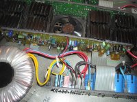
here is a foto. it shows a small pa - amp, the psu board (+v 0 -v) is connected with a "ribbon cable" to the poweramp boards (the +-15v are made with res and z-diodes on the preamp board).
here is a foto. it shows a small pa - amp, the psu board (+v 0 -v) is connected with a "ribbon cable" to the poweramp boards (the +-15v are made with res and z-diodes on the preamp board).
Attachments
Do things that would otherwise be impossible (without a multilayer PCB)!
Thanks.
That seems like a pretty difficult question for me to try to answer, for the general case (or for "the average audio power amplifier"). So I'll give it a try.
[Below is what I think, so far, but I do still need to examine the algebra and physics a little more closely to see if there are any major "gotchas".]
Competently using multiple parallel copies of power and ground rails in an audio power amplifier design should be able to result in (at least) lower Distortion and better Stability, plus better Transient Response characteristics. I can't think of any less-than-favorable effects that might occur. "How much better?", you might wish you could ask. It depends! But I'm guessing that it would at least be "significant", as in "not negligible".
You are asking something like the equivalent of, "What are the benefits of having smaller power-rail voltage fluctuations and lower power supply impedance and better decoupling/bypassing?".
The answer, in general, is, "It depends.".
But in at least some cases the benefits would probably seem relatively large compared to the benefits of many of the things to which a lot of diyaudio people devote much time, effort, and money.
For example, do you question why people worry about designing or using super-regulators, or why AndewT uses 75,000 uF (75 mF) of capacitance on each rail? (OK. maybe you do.)
I guess the typical answer is something like, "It might improve the sound.".
Most of the time, the improvement is not quantified, and sometimes its mechanism is not even well-defined or not known at all, and often the question of whether "might improve" actually did or did not improve is never even resolved.
I am trying to (eventually) actually quantify certain things, in this part of this thread. But even if I did eventually post all of the equations that could answer your question(s), the answer(s) would still depend on how (and how well) the techniques were applied, and would depend on in exactly what contexts they were used.
I thought about the possible "overkill" aspects, too. But the improvements in the example I gave seem quite dramatic for what are essentially trivial circuit-layout changes, requiring no additional components in most similar cases (and possibly fewer or cheaper components, in other cases).
So in some cases it might be overkill while in others it would be essential to make them even possible.
But the cost-benefit ratio should usually be favorable, since the cost would typically be low.
And "audiophile" stuff is basically all overkill, anyway, in one way or another, to somebody.
I would probably have to question why one _wouldn't_ use multiple parallel copies of power rail and power ground conductors, rather than why they would.
Its use should have significant good effects for a circuit designer to take advantage of, for most or all new power amplifier and preamplifier designs, and for many digital circuits (and for many other types of circuits).
Anyway, you might want to remember this technique, if/when you start designing decoupling networks mathematically, for example, or if you need the highest performance from decoupling capacitors and/or a power supply.
Without this paralleling technique, it can be literally impossible to hit the needed worst-case target impedance (as seen by the active device power pins) over the entire desired frequency range, even just as is required for relatively-slow devices such as chipamps.
That's probably the type of situation that would cause most commercial PCB layout designers to switch to using a multi-layer PCB with power and ground planes, if they weren't already using them. (But unless they know enough to distribute the power or ground feed through multiple connection points to each plane, for example, and distribute the capacitors in certain ways, then the multiple capacitor currents might still tend to all flow on top of each other, at least part of the time, negating some or all of the ESL reduction from paralleling. And in that case the discrete multi-parallel-conductor method being discussed here could actually be superior (in terms of capacitor and PCB trace ESL reduction), since by its very nature it basically _guarantees_ that parasitic inductances will be reduced by being paralleled, whereas when using planes that would still depend on using a correct layout to prevent the formation of mutual inductances among the parasitics, which wreck the algebra for the reduction that paralleling would otherwise induce.)
BUT, for our simple, cheap, home-made one-sided and two-sided DIY printed circuit boards (PCBs), and even for point-to-point wiring, we can gain at least ONE of the main benefits (of PCB planes) by using multiple parallel copies of power and ground rails, which will enable us to do things that would otherwise be impossible without a mutli-layer circuit board with power and ground planes and surface-mount components.
Well, let me start over and try again to answer your question:
Basically, the benefits are configurable. So everyone's mileage will vary.
It (multi-paralleling) can enable design of a better and/or easier-to-implement bypass and decoupling capacitor configuration, making it much easier and/or cheaper to meet a design target for, for example, (a low) maximum load-induced voltage-rail disturbance amplitude.
It can enable meeting a design target for, for example, a "maximum available instantaneous transient current slew rate", at all, or, with fewer or smaller decoupling capacitors.
It can enable more-easily/cheaply meeting a design target for, for example, (a low) maximum power supply impedance, over a specified frequency band.
In layman's (marketing) terms, "Like magic, it will convert your old dented six-cylinder van into an agile shiny new high-performance race car!". (Vroom! Vroom!) <grin>
The silence is the sound of the residual noise of your amplifier being powered by this idea.
I think it's just fine, except that it may be getting into overkill range and diminishing returns. How much would an average audio power amplifier actually benefit from a power supply like this?
Maybe a class D amp would significantly benefit from this.
Thanks.
That seems like a pretty difficult question for me to try to answer, for the general case (or for "the average audio power amplifier"). So I'll give it a try.
[Below is what I think, so far, but I do still need to examine the algebra and physics a little more closely to see if there are any major "gotchas".]
Competently using multiple parallel copies of power and ground rails in an audio power amplifier design should be able to result in (at least) lower Distortion and better Stability, plus better Transient Response characteristics. I can't think of any less-than-favorable effects that might occur. "How much better?", you might wish you could ask. It depends! But I'm guessing that it would at least be "significant", as in "not negligible".
You are asking something like the equivalent of, "What are the benefits of having smaller power-rail voltage fluctuations and lower power supply impedance and better decoupling/bypassing?".
The answer, in general, is, "It depends.".
But in at least some cases the benefits would probably seem relatively large compared to the benefits of many of the things to which a lot of diyaudio people devote much time, effort, and money.
For example, do you question why people worry about designing or using super-regulators, or why AndewT uses 75,000 uF (75 mF) of capacitance on each rail? (OK. maybe you do.)
I guess the typical answer is something like, "It might improve the sound.".
Most of the time, the improvement is not quantified, and sometimes its mechanism is not even well-defined or not known at all, and often the question of whether "might improve" actually did or did not improve is never even resolved.
I am trying to (eventually) actually quantify certain things, in this part of this thread. But even if I did eventually post all of the equations that could answer your question(s), the answer(s) would still depend on how (and how well) the techniques were applied, and would depend on in exactly what contexts they were used.
I thought about the possible "overkill" aspects, too. But the improvements in the example I gave seem quite dramatic for what are essentially trivial circuit-layout changes, requiring no additional components in most similar cases (and possibly fewer or cheaper components, in other cases).
So in some cases it might be overkill while in others it would be essential to make them even possible.
But the cost-benefit ratio should usually be favorable, since the cost would typically be low.
And "audiophile" stuff is basically all overkill, anyway, in one way or another, to somebody.
I would probably have to question why one _wouldn't_ use multiple parallel copies of power rail and power ground conductors, rather than why they would.
Its use should have significant good effects for a circuit designer to take advantage of, for most or all new power amplifier and preamplifier designs, and for many digital circuits (and for many other types of circuits).
Anyway, you might want to remember this technique, if/when you start designing decoupling networks mathematically, for example, or if you need the highest performance from decoupling capacitors and/or a power supply.
Without this paralleling technique, it can be literally impossible to hit the needed worst-case target impedance (as seen by the active device power pins) over the entire desired frequency range, even just as is required for relatively-slow devices such as chipamps.
That's probably the type of situation that would cause most commercial PCB layout designers to switch to using a multi-layer PCB with power and ground planes, if they weren't already using them. (But unless they know enough to distribute the power or ground feed through multiple connection points to each plane, for example, and distribute the capacitors in certain ways, then the multiple capacitor currents might still tend to all flow on top of each other, at least part of the time, negating some or all of the ESL reduction from paralleling. And in that case the discrete multi-parallel-conductor method being discussed here could actually be superior (in terms of capacitor and PCB trace ESL reduction), since by its very nature it basically _guarantees_ that parasitic inductances will be reduced by being paralleled, whereas when using planes that would still depend on using a correct layout to prevent the formation of mutual inductances among the parasitics, which wreck the algebra for the reduction that paralleling would otherwise induce.)
BUT, for our simple, cheap, home-made one-sided and two-sided DIY printed circuit boards (PCBs), and even for point-to-point wiring, we can gain at least ONE of the main benefits (of PCB planes) by using multiple parallel copies of power and ground rails, which will enable us to do things that would otherwise be impossible without a mutli-layer circuit board with power and ground planes and surface-mount components.
Well, let me start over and try again to answer your question:
Basically, the benefits are configurable.
So everyone's mileage will vary.It (multi-paralleling) can enable design of a better and/or easier-to-implement bypass and decoupling capacitor configuration, making it much easier and/or cheaper to meet a design target for, for example, (a low) maximum load-induced voltage-rail disturbance amplitude.
It can enable meeting a design target for, for example, a "maximum available instantaneous transient current slew rate", at all, or, with fewer or smaller decoupling capacitors.
It can enable more-easily/cheaply meeting a design target for, for example, (a low) maximum power supply impedance, over a specified frequency band.
In layman's (marketing) terms, "Like magic, it will convert your old dented six-cylinder van into an agile shiny new high-performance race car!". (Vroom! Vroom!) <grin>
Any means that force the loopcurrent-induced magnetic flux to travel ALL THE WAY through the smallest possible looparea will reduce inductance, stray and pickup of external fields. Reducing the loop area is the most efficient thing to do. Unluckely most caps are seldom built the way to accomplish that the best possible way.
- Status
- This old topic is closed. If you want to reopen this topic, contact a moderator using the "Report Post" button.
- Home
- Amplifiers
- Power Supplies
- paralleling film caps with electrolytic caps