Calculating values for decoupling capacitors:
The classic equation for capacitor behavior is
i = C dv/dt .
So we should be able to use
C = Ipeak (delta t / delta V)
where delta V is the desired or allowed maximum drop in voltage across the capacitor when we need Ipeak amps with a risetime of delta t seconds.
Another form of that equation is
C = (delta I) / (2 Pi f deltaV), where f is frequency.
We also know that the maximum derivative (aka slope, aka slew rate) for a sine wave is
slew rate max of sine (in volts per microsecond) = [(2 x Pi) x (freq in Hz) x (amplitude in volts)] / 1,000,000
So, for example, if one side of an amplifier can slew 20 V/us for 2 us, with a 4 Ohm load, that would be 10 amps in 2 us, and the minimum required decoupling capacitance should be
C = Ipeak (delta t / delta V) = 10 A x 2 us / delta V
If we choose delta V to be 0.1 Volt, then C = 200 uF.
The alternate equation involving f gives double that C value (for the corresponding f = 39.75 kHz) so it must be giving the total capacitance for both rails, assuming a rail-to-rail swing, or else I was off by a factor of two in my frequency calculation.
We also know that for an inductor,
V = L di/dt .
So we should be able to approximate that as
L = Vpeak (delta t / delta i)
which for the above case gives
L = 0.1V x (2 us / 10A) = 20 nH,
which should mean that there needs to be less than or equal to 20 nH of inductance, total, which would include at least the capacitor's internal inductance plus the inductance of the capacitor's leads, the pcb traces or wires, and the amplification device's power and ground leads, for the path that runs from the amp device through its power pin then through the cap and the amp's ground pin.
Using the rule of thumb that every inch of PCB trace has about 20 nH of inductance, and guessing about 5 nH for the capacitor's inductance, that would mean that the total round trip distance could only be 0.75 inch (about 18 mm), i.e. including the PCB traces and the amp device's power and ground leads!
For a better estimate of trace inductance, use Equation (2) at Analog Devices : Analog Dialogue : PCB Layout .
It also looks like an upper bound for the maximum ESR of the cap (ignoring voltage across the internal inductance of the cap, for the moment) could be
ESR < 0.1V/10A = 10 mOhms, at 39.75 kHz, for our example.
ESR changes significantly with frequency, but DF (dissipation factor) should stay within about a 2:1 ratio, typically.
DF (aka Tan(delta)) = 2.Pi.f.C.ESR
Here, still ignoring the voltage across the cap's internal inductance, an upper bound for DF for the 200 uF cap would be about
DF = 2 x Pi x 39750 x 200 x 0.01 = 0.50, for our example.
Since most electrolytics have ESR spec'd only at 120 Hz, we can calculate the ESR(120Hz) based on the DF and the ESR@39.75kHz, to get an upper bound for the ESR spec @ 120 Hz.
ESR = Df / ( 2.Pi.f.C) = 0.5/(2.Pi.120.200u) = 3.3 Ohms max @ 120 Hz, for our example.
Pulling a number out of the air for the capacitor's inductance, 5 nH, would give a voltage contribution across the cap of about
L x (delta i) / (delta t) = 5n.10A/2u = .025V, for our example,
leaving 0.075V to be induced across the ESR, if we want to maintain our chosen 0.1-Volt change across the capacitor.
That would give a max ESR estimate @ 39.75 kHz of 7.5 mOhms, giving a DF of 0.37, which would give an maximum ESR@120Hz spec of 2.45 Ohms. But since the DF could vary by a factor of 2 or so, it should be safer to look for a 200 uF capacitor with a maximum ESR of about 1.2 Ohms at 120 Hz.
Sorry if there are arithmetic or math (or other) errors. I was just making this up as I went.
I still need to simulate or test all of this stuff, to see if it's even close to being accurate.
Last edited:
Yeah, I think I used peak-to-peak amplitude to calculate the "equivalent frequency" from the max slew rate, when I should have used 0-peak amplitude. I still can't remember which way is correct but I'm guessing 0-peak is the "amplitude" that I used when deriving the max slew rate equation. So a bunch of stuff in the example might be off by a factor of either 2 or 1/2.
Last edited:
The matter of whether the example has an error of 2 or 0.5 can be sorted later.
What really matters, to me, is that the analysis shows that a 1us 10Apk signal can be supplied by a ~220uF cap, if esr and inductance are low enough.
By scaling we can see that a 10Apk 10ns pulse can be supplied by a 2uF cap. and similarly that a 10Apk 1ns pulse can be supplied by a 200nF cap wrapped very closely around the device terminals.
It's a beautiful thing, eh?!
(But I think it was a 2us, not 1us, 10aApk signal that could be supplied by a 200 uF cap.)
I received the Henry W. Ott book (Electromagnetic Compatibility Engineering, 2009 revised edition) in the mail, today, and when I first cracked open the 843-page book, it opened to the section on decoupling.
One immediate tidbit: Rise time and frequency are related by:
trise = 1 / (Pi f)
or
f = 1 / (Pi trise)
And, of course, the best decoupling will happen at the resonant frequency of the series capacitance and parasitic inductance, since the impedance will be at a minimum at that frequency, which is given by
f = 1 / ( 2 Pi sqrt( L C ))
For fun, I decided to combine those two equations, to try to get an equation for the "optimal" C value (impedance-wise, only) to use for a given rise time, given the total parasitic inductance. Substituting the expression for f from either equation into the other gives
C = ((trise^2) / 4) / L
For your 1 us trise example, that comes out to about C = .00025 / L , if L is in nH. It seems a little odd that we have to make L = 1.25 nH befoe it gives C = 200uF. But of course it blows up to infinity for L = 0. Unfortunately, for practical values of L, the C is relatively small. For example, with 30 nH, it would be about 8.33 uF.
----------------------
I haven't finished Ott's decoupling material, yet, but have read enough to see that using multiple identical decoupling caps is a good idea (and multiple different-valued caps can be bad). He's describing it in the context of digital circuit applications, but it looks more-broadly applicable.
Note that by paralleling n caps, the total capacitance is multiplied by n and the total inductance is divided by n, which are both in our favor. HOWEVER, the inductance will only divide by n if there is NO mutual inductance. That means that the "parallel" caps must not share the same conductors. They would either have to be connected by a "star" of sets of two conductors (all meeting across the power and ground pins to be decoupled), or be "spread out" and use power and ground planes.
We can take the allowable power supply rail transient voltage variation, dV, and the maximum transient current draw or current change, dI and calculate a target impedance,
Zt = dV/dI .
For our example of 10 Amps in 2 us with only 0.1 Volt of power rail disturbance amplitude, that would give Ztarget = 0.1V / 10A = 10 mOhms, which would need to be in place at least up to the f = 1 / (Pi trise) frequency of 159 kHz.
If we assume that each ideal capacitor has L = 30 nH in series with it, then according to Henry Ott we can calculate the minimum number of capacitors needed with
n = (2 L) / (Ztarget trise) (which, for our example, reduces to 0.1 x L, if L is in nH) = 3 capacitors .
Mr. Ott notes that one key to optimum decoupling design is knowing what inductance to use in the equation above.
Since the magnitude of the impedance of a capacitance is Z = 1 / (2 Pi f C), we can solve for C for a given Z (Ohms) and f as
C = 1 / (2 Pi f Z) .
Up to the frequency that is equivalent to the example rise time of 2 us, 159 kHz, we can calculate that in order to maintain our target impedance of 10 mOhms (0.010 Ohms), we would need a total capacitance of at least C >= 1 / (2 Pi 159k .01) = 100 uF
But below the resonant frequency, the capacitance must also be able to supply the transient current requirements,
C >= dI dt / dV ,
which for our example would be 10A 2us / 0.1V = 200 uF.
To satisfy both the impedance and transient current requirements, we would choose the larger capacitance of 200 uF and then divide by at least the minimum number of capacitors required, and would therefore need to use at least n = 3 capacitors of at least C/3 = 66.67 uF each.
So the answer (for an LM3886 with its 19 V/us typical slew rate, say 20 V/us, and up to 40 V power rails just to be safe, with a 4 Ohm load) would be:
qty (3) 68 uF capacitors, minimum, per rail,
assuming 30 nH total parasitic inductance for each cap and its connections to the power and ground pins. Remember, too, that the three decoupling capacitors should not share the same conductors, to connect to the power and ground pins, since that would make the total inductance not divide by the number of capacitors.
Of course, on the same board, there would also need to be "bulk capacitors" on each rail, totaling at least as much capacitance as the decoupling capacitors, and having low equivalent series inductance. The bulk capacitors are needed to recharge the decoupling capacitors between transient events. We might have to worry about low-frequency resonances, if the bulk capacitors are much larger in size than the decoupling capacitors. But if there is much ESR in the capacitors at the lower frequencies, it should help to damp any resonances.
Cheers,
Tom
Last edited:
Another good reference:
http://www.interferencetechnology.com/uploads/media/ITEM_01.pdf
PCB inductance:
http://www.polarinstruments.com/support/cits/IPC1999.pdf
Most if not all published figures for PCB inductance are based on a ground plane being present, as the return path is critical in calculating inductance.
I'm currently on pages 436 onward of Mr Otts book as we are looking into planar capacitance and whether we use to many power islands as shown in figure 11.22...or whether a uninterupted plane pair with planar capacitance would be better.
Last edited:
I am aware (very) aware of the impotance of the return path, but to calculate the inductance of a trace without a ground plane is more complex, inductance is of the loop, and with decoupling of digital signals or for RF decoupling the inductance loop is of paramount importance, you cannot calculate a PCb trace inductance without taking into account the return path, and if you dont have a ground plane the calculations are harder and the trace inductance will be higher. So for star grounded layouts as you often do on the amplifiers you realy need to use a 3D field solver such as those from polar intruments or simple calcs can be done using one or two of the options in the calculator before. The figure Gootee quoted is for a microstrip trace.
Inductance Calculator
http://www.speedingedge.com/PDF-Files/BTS006_What_Is_Inductance (2).pdf
Just out of interest I am also collating inductance figures for small (0603-0402) chip capacitors and there routing, as with moving to HDI (high density interconnect) we can halve the inductance for a placed and routed 0402 capacitor.
I'm sure that I made a lot of wrong assumptions and some errors. Still learning.
Yes, all of those calculations (above) are probably quite optimistic unless a ground plane is used.
With a one-sided PCB, probably the best we could do would be to put two traces as close together as possible. And even then, the characteristic impedance (sqrt(L/C)) won't get below a hundred Ohms. e.g. Two flat conductors, .0027 inch thick, each 0.020 inch wide, separated by 0.04 inch, on a glass-epoxy PCB, would have a characteristic impedance of 120 Ohms. For our power distribution loops we would rather have 1 Ohm or less!
And THAT'S one reason that we need decoupling capacitors. They make a power/ground pin pair see a low impedance supply of current.
Also note that without a low-impedance DC power rail, the voltage noise induced across the power rail impedance by time-varying current demands could feed into the amplifier input, which could cause oscillation. (Imagine a simple transistor amplifier and the resistors from rail to transistor base and base to ground. Power and ground rails are coupled to amplifier input, there.) So we basically need to provide a short circuit for AC from rail to ground, across the entire band at which the amplifier has gain, to avoid having voltage disturbances feed into the amplifier's input. Our decoupling capacitors should also provide that. That's also another good reason to use a low-pass input filter, if the amplifier has gain at frequencies past what we need.
I still need to do some more learning, and simulations and experiments, to better understand how we might be able tio apply these types of concepts and calculations to simple DIY configurations.
I am hoping that someone who already knows will jump in. I'm already imagining having to arrange and solder a dozen small electrolytic decoupling capacitors like the pistons in a twelve-cylinder radial aircraft engine and then solder two leads from the assembly to my board.
Last edited:
I do a lot of high speed and mixed signal layout, where I always use a ground plane or several, most of my boards being 6 layers (analogue/digital) to up to 16 layers, high speed digital, so the calculators etc are all geared up for these type of designs. Also because of EMC etc and historical reasons all analogue boards I do have a ground plane of some sort, even audio boards. For most designs I would promote a contiguous ground plane, but on SMPS , audio and harmonic motor control boards the ground is split into sections (power, low level signal) quite often by different layers or strategic moats to control the current flow of either the high power returns (audio amps and motor control) or switching loops (SMPS's). Because of the increasing speed, density fast rise time etc of today's electronics, the integrity of the power delivery system is becoming more critical, and the more reading I do on the subject the more I find I have to understand. in my case I am luckier than some as I have quite extensive software tools for signal integrity as part of my CAD system, and for my PCB's, I can get impedance and inductance reports from the PCB manufacturers I use...also I can get things EMC tested so I see in quite intimate details what happens and what effect my layout has on these things (and if I get something wrong, the details get really intimate).
The technick calculators have co-planar and vertically spaced sections which should give approximations for star grounded layouts.
Its a great subject to study as its changing and becoming more challenging as rise times, clock speeds and wideband EMC noise increase.
The technick calculators have co-planar and vertically spaced sections which should give approximations for star grounded layouts.
Its a great subject to study as its changing and becoming more challenging as rise times, clock speeds and wideband EMC noise increase.
Some PDfs etc of power point displays that should be of interest:
http://www.pcbcarolina.com/images/01_PCB_Power_Decoupling_Myths_Debunked.pdf
Decoupling
http://www.ewh.ieee.org/r4/se_michigan/emcs/DL-ARCH-decoupling3.pdf
http://web.mst.edu/~jfan/slides/Archambeault1.pdf
http://www.ece.rochester.edu/users/friedman/papers/TVLSI_06_Decap.pdf
http://www.pcbcarolina.com/images/01_PCB_Power_Decoupling_Myths_Debunked.pdf
Decoupling
http://www.ewh.ieee.org/r4/se_michigan/emcs/DL-ARCH-decoupling3.pdf
http://web.mst.edu/~jfan/slides/Archambeault1.pdf
http://www.ece.rochester.edu/users/friedman/papers/TVLSI_06_Decap.pdf
Were having fun here at work, looking at the differences between multiple values vs single value, and low q vs high q. Hoping to do a test board so we can see the differences for ourselves, as we have differing views between engineers.Using low Q MLCC X7R capacitors has help keep resonant peaks down as we have tended towards decade resistors 100n 10n 1n.
Thanks for re-vitalising my interest in this subject, for some reason a lot of people find it rather dry and uninteresting here!!!
Thanks for re-vitalising my interest in this subject, for some reason a lot of people find it rather dry and uninteresting here!!!
this advice (or very similar) has been posted many times on the Forum. But many Members have repeatedly refused to believe it..........Using low Q MLCC X7R capacitors has help keep resonant peaks down......
They need to argue with Henry Ott and Bruce Archambeault
Its the same in the seedy world of electronic design, no two engineers can agree on deoupling and many wont read the reports and research out there, but rely on their beliefs.
I use to be a proponent of multiple values to get broad band decoupling, now I would like to do some experiments to see for myself (and the rest of us) the difference between multiple values and the same value...
We have a couple of EMC spikes that are not directly related to clocks (they may be a harmonic) that may be due to the frquency being at one of the anti-resonance peaks.
Correct. You can soften differential microstrips burying them (e.g. covering with soldermask) and by increasing trace width but the dominant effect is the gap width. Saturn PCB's toolkit includes impedance calculators for a variety of trace geometries. You may want to download it and fool around to get a sense of the numbers and how they behave as you vary the geometry.With a one-sided PCB, probably the best we could do would be to put two traces as close together as possible.
It's a good rule of thumb a well implemented differential pair is 100 ohms. Somehow, just about every manufacturing process for making them works out that way.
If your bypassing is an electrically large distance away from the load---so that the supply behaves as a transmission line---you have bigger problems than the supply's characteristic impedance. That routing geometry's something like 20nH/inch, so you're correct it rapidly becomes painful in the more typical case where a lumped model applies to an electrically small supply.Two flat conductors, .0027 inch thick, each 0.020 inch wide, separated by 0.04 inch, on a glass-epoxy PCB, would have a characteristic impedance of 120 Ohms. For our power distribution loops we would rather have 1 Ohm or less!
Happens all the time with people who haven't learned about bypassing yet. I posted an analysis of the consequences of inductance in a well designed supply over here.Also note that without a low-impedance DC power rail, the voltage noise induced across the power rail impedance by time-varying current demands could feed into the amplifier input, which could cause oscillation.
Not much point. The caps are in packages with a few nH of ESL---put as many of them in parallel as you want but you won't reduce that---and you'll get more nH from the leads. If you want a low inductance supply you need to be thinking MLCCs next to the chip pins. The industry standard for analog designs is 100nF X5R or X7R---for DIY usually 0603 or 0805 packages work well.I'm already imagining having to arrange and solder a dozen small electrolytic decoupling capacitors like the pistons in a twelve-cylinder radial aircraft engine and then solder two leads from the assembly to my board.
Have a look at the July 24, 2006 presentation here for ideas. Other things being equal, caps limit on ESR on ESL. Larger packages are lower ESR but somewhat higher ESL so it's just a tradeoff as to what gives the lowest impedance at the frequencies of interest. Of course, other things aren't equal and, in practice, what I find is if you're really counting milliohms on the supply impdeance you're trying to get as many wide/X2Y MLCCs and vias as close to the part as you can while still being able to route the signals out of the chip and not obliterating the planes with all the vias---that link provides a good illustration of life with a package that's a couple hundred pH when vias are a few hundred pH each.I use to be a proponent of multiple values to get broad band decoupling, now I would like to do some experiments to see for myself (and the rest of us) the difference between multiple values and the same value...
I'm not too much a fan of decade resistors due to the cost in board space. For example, if you're working 0402 and do 1 || 10 || 100nH you're presumably putting a 1nF cap with around 600pH ESL next to the part when you could have just put the 100nF with around 500pH ESL next to the part to start with. ESR on the 100nF's a few mOhm lower, too. One obviously has to sim the layout out and then validate with measurements, but doing something like 100 || 100nH and using the board area freed up from getting rid of the third cap for doubling up vias on each cap (to cut off a few hundred more pH) is likely to work out to a lower supply iimpedance with a lower BOM cost and more energy stored close to the part.
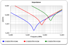
The resonances on the 1 and 10nH do pull a hundred mOhm or a few hundred mOhm lower than the 100nH's ESL limit. But up around 100MHz 100pH is around 100mOhm on the supply so it's really the vias that matter. Get towards 1GHz---above resonance on the smaller caps---and the 100nF's lower ESL wins. That said, if you've a problem EMI peak then placing some caps whose resonance lands near the peak can be a useful narrowband optimization to knock it down a bit. To save you the hassle of looking up the 0402 X7R TDK part numbers in the attachment, blue is 100nH, red is 10nH, green is 1nH.
One of the nice things about DIY hand soldering is you can do via in pad without worrying about tombstoning the part.
Attachments
Never had a problem with tombstoning, luckily.
Looked at the XY2 caps as well as other low inductance designs, such as multiple caps in BGA packages.
Limited with numer of vias that we can get on the capacitors, these are boards covered in BGA's with DDR2 ram (not DIMM modules), double sided placement, IPC class 3, 3500 plus component pins in a board 100mm x85mm 12-16 layers (sig next to contigous ground plane, dont allow vias to create slots either)! Next step is HDI:
Microvia HDI
I am currently changing one of the design to HDi, the via in pad with the 1005 (0402) resistors halves the inductance. plus going to use planar capacitance with closely spaced power pairs.
The choice of multiple values is not mine, the engineer makes that choice, which is why I get boards with several decoupling stratergies for different areas of the design but as can be seen from below, they are all 0402 and all are placed below the BGA pads (1mm pitch BGA, when you get 0.8 and smaller it becomes more of a pain) so it is just a case of changing the BOM and placement data to use just one value, then run EMC tests etc.
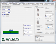
The Saturn impedance toolkit, all options have a ground plane present...
As for hand soldering or even looking at boards, I am at the age where 25+ years in front of a monitor means that its all just one big blur, without some serious magnification, thank goodness for the Zoom function in CAD, and when you get to 0201 capacitors, its like a bag of fairy dust.
The PCB area shown is approx 7mm x 8mm in the real world.
Looked at the XY2 caps as well as other low inductance designs, such as multiple caps in BGA packages.
Limited with numer of vias that we can get on the capacitors, these are boards covered in BGA's with DDR2 ram (not DIMM modules), double sided placement, IPC class 3, 3500 plus component pins in a board 100mm x85mm 12-16 layers (sig next to contigous ground plane, dont allow vias to create slots either)! Next step is HDI:
Microvia HDI
I am currently changing one of the design to HDi, the via in pad with the 1005 (0402) resistors halves the inductance. plus going to use planar capacitance with closely spaced power pairs.
The choice of multiple values is not mine, the engineer makes that choice, which is why I get boards with several decoupling stratergies for different areas of the design
but as can be seen from below, they are all 0402 and all are placed below the BGA pads (1mm pitch BGA, when you get 0.8 and smaller it becomes more of a pain) so it is just a case of changing the BOM and placement data to use just one value, then run EMC tests etc.The Saturn impedance toolkit, all options have a ground plane present...
As for hand soldering or even looking at boards, I am at the age where 25+ years in front of a monitor means that its all just one big blur, without some serious magnification, thank goodness for the Zoom function in CAD, and when you get to 0201 capacitors, its like a bag of fairy dust.
The PCB area shown is approx 7mm x 8mm in the real world.
Attachments
The theory behind bypassing electrolytics with very low capacitance film caps is that at very low voltages the larger value electrolytic cap will not exhibit the charactistics of a true capacitor and will not properly handle low level signals. Personally I don't buy it but that's the theory behind it. It's most frequenly used in series capacitors in crossover networks in the midrange and tweeter high pass sections.
The poster who said the voltage rating should exceed the maximum operating voltage of the circuit is correct. This is true for any capacitor in any circuit.
The poster who said the voltage rating should exceed the maximum operating voltage of the circuit is correct. This is true for any capacitor in any circuit.
That's a nice hot rod of a process, marce. Agree you're pretty much up against whatever the BGA pinout provides without blind vias, though a backside array of pin straddling MLCCs is pretty darn decent. One can do some fine tuning by spreading a range of caps and, if the process supports it, cutting out some of the layers to shorten the vias. Mostly you're just staring physics in the face though. The fairy dust option is nice though; some people do it, but I wouldn't want to be hand soldering a lot of 0201s. In DIY land I'm mostly working with 0603 on Gold Phoenix's base process in two layers, occasionally four. Makes dealing with things like a DAPped QFN kind of interesting, though at least I know I can put plenty of solder down with a hot iron. Means I can pull the caps' GND pads under the package in a backside assembly and flood them for the thermals. No shortage of GND vias but getting 25 mil Vdd vias in on 0.5mm pitch part's not exactly trivial.
Agree you're pretty much up against whatever the BGA pinout provides without blind vias, though a backside array of pin straddling MLCCs is pretty darn decent. One can do some fine tuning by spreading a range of caps and, if the process supports it, cutting out some of the layers to shorten the vias. Mostly you're just staring physics in the face though. The fairy dust option is nice though; some people do it, but I wouldn't want to be hand soldering a lot of 0201s. In DIY land I'm mostly working with 0603 on Gold Phoenix's base process in two layers, occasionally four. Makes dealing with things like a DAPped QFN kind of interesting, though at least I know I can put plenty of solder down with a hot iron. Means I can pull the caps' GND pads under the package in a backside assembly and flood them for the thermals. No shortage of GND vias but getting 25 mil Vdd vias in on 0.5mm pitch part's not exactly trivial.Off the top of my head I recall there's a buried differential pair without planes. Maybe another one or two planeless. Though most of the field's carried directly under the trace. So most of the plane can be removed with too much stiffening of the impedance.The Saturn impedance toolkit, all options have a ground plane present...
- Status
- This old topic is closed. If you want to reopen this topic, contact a moderator using the "Report Post" button.
- Home
- Amplifiers
- Power Supplies
- paralleling film caps with electrolytic caps