I want to take the opportunity to appeal to the inventors and designers of
(all) circuits called Paradise Phono :
Reliable links to valid schematics, bill of material, board layout and build
instructions should finally be provided and good pictures added. It is always
possible to edit the first post of any thread for this purpose. As is, the
distributed documentation of this project is a discouraging mess and the
schematics are ugly.
Please check here: https://www.diyaudio.com/community/threads/paradise-builders.218625/post-3189527
This is the link to the R3 documents, so I hope that this helps you. But I am glad to see you fixed this already by yourself, thanks! My apologies I saw these posts too late, I should have looked earlier.
Enjoy!
In my experience this is not complete and easy enough to work with for the users.
Have a look at the schematic - it is a mess. Also, there is a different version with bjt
output. Of the regulator I see also (at least) two versions. Schematics have part
numbers, pcbs not.
I asked for a set of complete information with all changes. This would it make easier
to help others. The assembly guide does not have big clear pictures. Picture in the
guide sais "R2" (p. 6).
etc
Yes, I understand. Remember the R3 version was the one that was produced in volumes (700 PCBs, if I remember correctly). The R1 never went public, and the R2 only went to a handful of people who were going to be beta builders, for testing. The Calvin Buffer output stage came later, after release of R3, and was designed to fit on top of the R3 PCB. So the "official" version is R3. And this thread is supposed to be the place for people to ask questions with their builds, which is apparently happening very well (despite little traffic in the last years). Many happy Paradise owners out there 
My point is that all relevant information should be in a single post, easy to find for everybody,
this would be post 1 of an existing or new thread. In the picture in post 4465 you see that the
Jfet buffer is on board, not on top. We can not know how many successful builds have been made.
this would be post 1 of an existing or new thread. In the picture in post 4465 you see that the
Jfet buffer is on board, not on top. We can not know how many successful builds have been made.
I see that I requested this already six years ago :
https://www.diyaudio.com/community/threads/mpp.154210/page-548#post-5439782
https://www.diyaudio.com/community/threads/mpp.154210/page-548#post-5439782
So I picket up a Beta Version with my R2 boards. Lucky me !
Might explain why they are so hard to complete.
board #1 works fine.
Now struggling with the second one. Layout is a pain to solder.
Pin 6 of the opamp -18V, output voltage and voltage at the ext Riaa close to 18V.
Transistors at the side of the opamp (337s) get really hot.
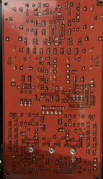
And here‘s the picture of the soldering side.
!Might explain why they are so hard to complete.
board #1 works fine.
Now struggling with the second one. Layout is a pain to solder.
Pin 6 of the opamp -18V, output voltage and voltage at the ext Riaa close to 18V.
Transistors at the side of the opamp (337s) get really hot.
And here‘s the picture of the soldering side.
Attachments
Posting from new account.
I don't know how many have been built, but I've scratch built over 40 for various people and finished at least a dozen more that were incomplete of built wrong for other people.
I've read every post on all the paradise threads and only ever seen maybe two guys give up.
I reckon I've seen every mistake you can think of, and in order of frequency, bad solder work, 327 and 337 swapped or one fitted backwards, bad input stage matching such that the shunt voltage supply is hard up against the current limit the opamp is maxed out and one rail is stuck around 7V. One thing to note is that mixing input stage transistors across different brands is a bad move, they might match for current gain on a peak meter, but under operating conditions the forward transconductance is way out.
And while we're at it. The caps either side of the shunt should be 30v minimum, and the 2 pairs of nichicon caps 10/100uf need to be 25v not the 16v supplied in the parts kit. For the 10uf caps use 10uf/35v Panasonic FC to get the required higher esr needed fir stability in the shunt. Also ditch the 3.3k resistor, replace with 1k and replace j310 next to it with j113, on both sides.

Thx for looking so close @ste but those points are actually ok. I had to scratch the surface in order to be able to solder them.
@Simon1972 I read the assembly guide for R2 again and it states that R43a and b may be reduced from 150k which is what I‘ve did. (Resistors can hardly be removed from the board w/o breaking them btw.) They are now 125k which allows me to set the output voltage to somewhere between -1v and 1v within only a few degrees of the potentiometer. Input voltage will then be around 4v and opamp Pin 6 Close to 17v.
transistors are not getting hot anymore.
Something still very wrong here.
Stephan, did you zero the input offset voltage? I use 100r across input/gnd to do this. Once you've done it you'll need to readjust the two trimmers on the shunt to get an even +/- 18v. If you can't get +/- then I'd check all soldering, check all 327 337 are correct orientation and none placed incorrectly.
If that's all good then it's down to bad parts matching. If you're building from a supplied parts kit chances are you'll never get a good matched set.
If that's all good then it's down to bad parts matching. If you're building from a supplied parts kit chances are you'll never get a good matched set.
@Simon1972 thx for reminding me of the resistor across the input!
I was so focussed on the output voltage that I entirely forgot about it.
I've now increased R43a and b to 135k to ha ve a bit more freedom on the potentiometer wich worked quite well. I'm now at 0.020V on the output and 0V on the input with 100Ohm across it. Pin 6 on the opamp is somewhere near -4V which seems to be fairly ok I suppose.
Unfortunately I don't have any decend resistors near 135k lying around as I used trim-pots that I still had.
But that's probably an easy problem to solve.
So thank you for supporting me!
-4v is OK. I generally shoot for better than 0.5v but that takes a lot of swapping transistors. I usually solder 3 header pins into each end of the input stage so I can swap out the last parts.
So now that they're built, leave them powered up for about 70 hours. Seems crazy, but you can literally watch the output offset drop every couple of hours as the lytics form fully. Shoot me an address and I'll send you a set of input stage houses.
https://flic.kr/p/2mb83XA
So now that they're built, leave them powered up for about 70 hours. Seems crazy, but you can literally watch the output offset drop every couple of hours as the lytics form fully. Shoot me an address and I'll send you a set of input stage houses.
https://flic.kr/p/2mb83XA
@Simon1972 hopefully by tomorrow I will receive the resistors That will replace my trimpots.
Once soldered in I can start the burn in phase.
Not saure if the housings will fit as I have the R2 boards that are a bit different in layout.
Once soldered in I can start the burn in phase.
Not saure if the housings will fit as I have the R2 boards that are a bit different in layout.
- Home
- Source & Line
- Analogue Source
- Paradise Builders