hi there,
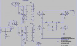
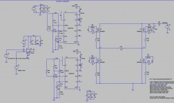
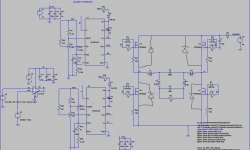
I'm designing a class d amplifier using IRF6645 transistor and IRS20124S mosfet driver with full bridge topology. I'm using pwm as modulator. you can see simplified schematics attached.
My problem is about the output transistors. When I connect single 8 ohm resistor as load, the circuit can operate @100W and output transistors' maximum temperature is about 65C degree and steady. When I connect a filter suitable for 8 ohm load and then operate again @100W, the output transistors' temperature continuously increase more than 100C degree in a short time.
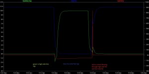
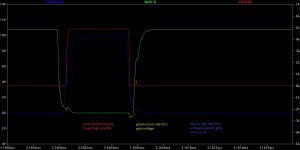
I can't understand the reason of this situation. I made 2 seperate simulation by using resistor as a load and filter+resistor as load with exact models of the fet driver and fets in both simulations as you can see in attached pictures. In the simulation that single resistor as load, there is no shootthrough current, but there is shootthrough when I connect filter+resistor as load. Is that possible inductive characteristic of the filter cause shootthrough and heats the transistor more?
or another reason, comes to my mind,(may be not logical) the reactive power heats the transistors. is that possible?
this made me sick. I couldnt find the reason why the transistor heats more and more when I changed the load. May be some of you confront with the same situation and survive it, can give me some idea or another aspect for solution..
this is my first class d design and my questions can seem easy but I'm struggling here..
I'm designing a class d amplifier using IRF6645 transistor and IRS20124S mosfet driver with full bridge topology. I'm using pwm as modulator. you can see simplified schematics attached.
My problem is about the output transistors. When I connect single 8 ohm resistor as load, the circuit can operate @100W and output transistors' maximum temperature is about 65C degree and steady. When I connect a filter suitable for 8 ohm load and then operate again @100W, the output transistors' temperature continuously increase more than 100C degree in a short time.
I can't understand the reason of this situation. I made 2 seperate simulation by using resistor as a load and filter+resistor as load with exact models of the fet driver and fets in both simulations as you can see in attached pictures. In the simulation that single resistor as load, there is no shootthrough current, but there is shootthrough when I connect filter+resistor as load. Is that possible inductive characteristic of the filter cause shootthrough and heats the transistor more?
or another reason, comes to my mind,(may be not logical) the reactive power heats the transistors. is that possible?
this made me sick. I couldnt find the reason why the transistor heats more and more when I changed the load. May be some of you confront with the same situation and survive it, can give me some idea or another aspect for solution..
this is my first class d design and my questions can seem easy but I'm struggling here..
Attachments
I think, you mean the situation high side mosfet's turn on when the body diode still conducting, I searched for some tricks preventing this situation, but the ways I found like using faster (low recovery charge) diodes than body diode of transistor is inefficient. if somebody know better ways of preventing diode and transistor conducting at the same time pls let me know thanks
'Bout shoot-through
The answer is Yes, You can.
You should generate so-called "deadtime" beforehand.
is it possible to prevent this shoot through current?
The answer is Yes, You can.
You should generate so-called "deadtime" beforehand.
Hi denniz..
I tried shunt diode, I used 1N4148 as shunt diode, but it didnt work neither in simulation nor in real board.may be 1N4148 was wrong choice, I preferred it because of its low Trr. I read other topics about body diode problems and I learned that Vf and Qrr important parameters. and I thiink 1n4148 is better than 1N5400 in this way. If you can explain why you advise 1N5400 I'll be glad.
thnx
thanks for the quick answer I'll look for "diode recovery charge" title but can you gıve some detailed explanation pls. how can reactive load heats transistors? reactive current return back to the supply so no enegy loss.. Am I wrong?
The power on the load/filter can be reactive, but not on the MOSFET! MOSFET is resistive, so any type of current creates real power (loss) on it.
I think, you mean the situation high side mosfet's turn on when the body diode still conducting,...
I'm glad you found some information!
...is it possible to prevent this shoot through current?...
Only a schottky has small enough Vf to carry the majority of the current, but I'm not sure if it's the best solution, because it has a relatively high capacitance. Try it!
The other solution can be the setting of minimal dead time. The channel can carry quite high current below Vf. If you turn on the other MOSFET exactly when the first MOSFET turns off, the diode doesn't have time to build up stored charge. Not an easy task in reality...
An other important factor is switching speed. The faster you want to switch off a diode the higher the Qrr is. You can play with turn on speed of MOSFET.
And finally: sometimes you have to accept that a loss cannot be eliminated. Then increase cooling!
Last edited:
Pafi thank you very much for the explanation. I had already accepted the loss but in simulation I saw nearly 100A current spikes through the transistors. this looks big stress on transistor and risky. I'm struggling because of this.
by the way I didnt see 100A current spikes (nearly 10A spike) through transistors on the real circuit but I thought because of the capacitance of the probe I missed the sharp spikes!? is that possible?
thanks again for the explanation I will try the ways you adviced
by the way I didnt see 100A current spikes (nearly 10A spike) through transistors on the real circuit but I thought because of the capacitance of the probe I missed the sharp spikes!? is that possible?
thanks again for the explanation I will try the ways you adviced
Currently I'm using IR IGBT along with 1N5400 with a full success and going to try out copacs as a next step.
So...
... Should be explained, suppose.
So...
1N5400 must be a joke, but not a good one. IGBT and dead time also.
... Should be explained, suppose.
hi there,
My problem is about the output transistors. When I connect single 8 ohm resistor as load, the circuit can operate @100W and output transistors' maximum temperature is about 65C degree and steady. When I connect a filter suitable for 8 ohm load and then operate again @100W, the output transistors' temperature continuously increase more than 100C degree in a short time.
I've had the same story with my very first trial and after all ran out of that using:
1. 2110 instead of 20124 (more control can be done)
2. According "deadtime" scheme (took one used in Crest 3000)
3. Putting "power" diods as recovery ones
One mention: All above is imperical consequence.
Ah, and PWM I used was just 20 kHz.
Currently I'm using IR IGBT along with 1N5400 with a full success and going to try out copacs as a next step.
So...
... Should be explained, suppose.
I don't think such an evident thing should be explained, but if you wish:
1N5400 is not fast at all, it's standard recovery diode, probably much slower then the body diode of IRF6645. Vf (@8A) is also higher then IRF6645. So it is absolutely not OK.
IRGB4045 is also worse than IRF6645 in almost every aspect: much higher conduction loss, slower diode, much slower turn off... the only benefit is higher VCE, but it is not needed.
You can use almost anything, with some results, but here the question was not just a not exploding device, but a better solution than the original (which is already quite good)!
Ah, and PWM I used was just 20 kHz.
20 kHz says: there are problems with your design. If you had been reached low switching loss (and proper EMC), you could have used much higher freq. with better result. A modern amplifier shouldn't run under 100 kHz even if it's only for sub.
And finally: sometimes you have to accept that a loss cannot be eliminated. Then increase cooling!
I had already accepted the loss but in simulation I saw nearly 100A current spikes through the transistors. this looks big stress on transistor and risky. I'm struggling because of this.
by the way I didnt see 100A current spikes (nearly 10A spike) through transistors on the real circuit but I thought because of the capacitance of the probe I missed the sharp spikes!? is that possible?
Pafi thank you very much for the explanation. I had already accepted the loss but in simulation I saw nearly 100A current spikes through the transistors. this looks big stress on transistor and risky. I'm struggling because of this.
by the way I didnt see 100A current spikes (nearly 10A spike) through transistors on the real circuit but I thought because of the capacitance of the probe I missed the sharp spikes!? is that possible?
thanks again for the explanation I will try the ways you adviced
You're welcome!
The lower current spikes can be caused by stray inductance and band-limited current probe also. What is your current probe? (I have only a homemade transformer, unable to measure over 50 MHz.)
Stray inductance in source connection can slow down current slope very effectively. For example Vg=10V, Vgs=5V, Ls=5 nH means 1000 A/ns. trr=31ns @ 100 A/ns, but slightly decreases with current slope rate, so maybe it's only 18 ns. trr=ta+tb, where ta is the time when current rising (fully opened p-n junction), and this time is maybe less then 10 ns, so current spike may be below 10 A, as you measured. But I guess it's a little more in reality.
I don't think such an evident thing should be explained, but if you wish:
1N5400 is not fast at all, it's standard recovery diode, probably much slower then the body diode of IRF6645. Vf (@8A) is also higher then IRF6645. So it is absolutely not OK.
IRGB4045 is also worse than IRF6645 in almost every aspect: much higher conduction loss, slower diode, much slower turn off... the only benefit is higher VCE, but it is not needed.
You can use almost anything, with some results, but here the question was not just a not exploding device, but a better solution than the original (which is already quite good)!
20 kHz says: there are problems with your design. If you had been reached low switching loss (and proper EMC), you could have used much higher freq. with better result. A modern amplifier shouldn't run under 100 kHz even if it's only for sub.
Thank You very much for an explanation, Pafi.
You're absolutely right in every aspect!
The only thing is "body diod" - doesn't it is just a parasitic PN structure inside a transistor?
So, why should one rely upon this "diod" as recovery one?
You're welcome!
The lower current spikes can be caused by stray inductance and band-limited current probe also. What is your current probe? (I have only a homemade transformer, unable to measure over 50 MHz.)
Stray inductance in source connection can slow down current slope very effectively. For example Vg=10V, Vgs=5V, Ls=5 nH means 1000 A/ns. trr=31ns @ 100 A/ns, but slightly decreases with current slope rate, so maybe it's only 18 ns. trr=ta+tb, where ta is the time when current rising (fully opened p-n junction), and this time is maybe less then 10 ns, so current spike may be below 10 A, as you measured. But I guess it's a little more in reality.
I use tektronix p2220 voltage probe to see the current pass through 0.1ohm resistor (as you can guess resistor is between the supply and transistors). I'm not using current probe.
As you say there may be measurement errors to see the real current values.
because of this I cant understand the techniques, I applied to reduce the spikes, is vital or not...
by the way as you said in previous message irf 6645 has a fast body diode so applying shunt diode technique is useless I think because I couldnt find a diode that has better power and timing specs and lower Vf?!
1N5400 is not fast at all, it's standard recovery diode, probably much slower then the body diode of IRF6645. Vf (@8A) is also higher then IRF6645. So it is absolutely not OK.
To conclude:
1. Leaving a design without recovery diod, one increases, let's say, power dissipation across transistor - that is an answer to Volcantr's very initial question, suppose.
2. 1N5400 just works and it shows on oscillogram and power transistors temperature substantial decrease - why should one ask for more?
3. Overall, when one TESTS a device for a minute or so and when the same device RUNS for an hour - the power reserve, that IGBTs along with robust recovery diod give, conquers all. Imperical fact, either.
But, should be added, that currently I'm on the very curious way to try a TRUE "Transistor plus Diod" structure from IR - they call it "copac".
You're welcome!
The lower current spikes can be caused by stray inductance and band-limited current probe also. What is your current probe? (I have only a homemade transformer, unable to measure over 50 MHz.)
Stray inductance in source connection can slow down current slope very effectively. For example Vg=10V, Vgs=5V, Ls=5 nH means 1000 A/ns. trr=31ns @ 100 A/ns, but slightly decreases with current slope rate, so maybe it's only 18 ns. trr=ta+tb, where ta is the time when current rising (fully opened p-n junction), and this time is maybe less then 10 ns, so current spike may be below 10 A, as you measured. But I guess it's a little more in reality.
Btw I tried shunt diode by using SS26 and MRA4007T3G diodes seperately (these diodes may be not suitable again but I have only these parts now) and it didnt work.
I played with the gate resistors and increase it near 33ohms but again it didnt work.. one last way, playing with dead times, may be it will work but now the mosfets increadibly hot! If I execute the circuit after 1 munites, the fets are smoking (without cooler) is that normal? only placing a cooler can be solution? it seems a bit risky to me. With single resistor as load with the same conditions it works with no problem (no cooler again)
Also I wonder, there is a lot of application "full bridge drive with inductive(reactive) load". Is everybody confronts with the same issues? may be I'm struggling at the false floor.?
I feel like loosers
") but for the last two weeks.. I'm struggling with this and I couldnt go forward a teeny step
but for the last two weeks.. I'm struggling with this and I couldnt go forward a teeny step- Status
- This old topic is closed. If you want to reopen this topic, contact a moderator using the "Report Post" button.
- Home
- Amplifiers
- Class D
- Output transistor temperature changes with load characteristics..